HCA-S Silicon and InGaAs Photoreceivers
- Technology
- Photodetectors
- Partner
- FEMTO Messtechnik
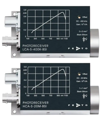
The HCA-S series converts small optical signals into proportional voltage signals using an integrated photodiode and fixed-gain transimpedance amplifier. DC-coupled bandwidth choices of 20, 200 and 400 MHz allow engineers to balance gain, noise, rise time and optical saturation power. Si-PIN versions cover visible and near-infrared wavelengths, with spectral ranges beginning at 320 nm. InGaAs-PIN models operate from 900 to 1700 nm and support near-infrared measurements, including applications at 1550 nm. The HCA-S-20M-BSI-FST black-silicon model provides an additional spectral range of 200 to 1100 nm.
Typical applications include spectroscopy, pulse and transient measurement, optical triggering, digital fibre-system testing and optical front ends for oscilloscopes or A/D converters. Threaded free-space and fixed FC input configurations support integration into optical benches and fibre-coupled systems.
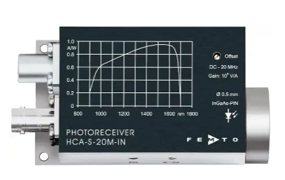
Range features
A high level overview of what this range offers
- 20, 200 and 400 MHz bandwidth options – Allow response speed to be matched to pulse, transient and modulated-light measurements.
- Fixed transimpedance gains from 5 × 10³ to 1 × 10⁵ V/A – Provide defined optical-current-to-voltage conversion for each bandwidth class.
- Si-PIN and InGaAs-PIN detector options – Cover wavelengths from 320 to 1700 nm across the main range.
- Black-silicon detector option – Extends the available spectral coverage to 200–1100 nm at 20 MHz.
- NEP from 3.3 pW/√Hz – Supports detection of low optical signal levels when measurement bandwidth and wavelength are considered.
- FST and fixed FC input configurations – Accommodate free-space optical arrangements and permanent fibre connections.
- 1.035″-40 threaded FST flange – Accepts compatible optical accessories and optional FC or FSMA fibre adaptors.
- Adjustable input offset compensation – Helps prevent background photocurrent or detector offset from consuming the available output range.
- 50 Ω BNC signal output – Supports connection to oscilloscopes, digitiser inputs and other 50 Ω measurement equipment.
- M4 and UNC 8-32 mounting threads – Enable installation on metric or imperial optical posts.
- Output short-circuit protection – Reduces the risk of output-stage damage during connection and set-up.
Downloads
for HCA-S Silicon and InGaAs Photoreceivers
What’s in this range?
All the variants in the range and a comparison of what they offer
Specifications
| Specification | HCA-S series data |
|---|---|
Product type | Fixed-gain DC-coupled photoreceiver |
Detector technologies | Si-PIN, InGaAs-PIN and black silicon |
Combined spectral coverage | 200–1700 nm, depending on detector option |
Bandwidth options | DC–20 MHz, DC–200 MHz or DC–400 MHz |
Transimpedance gain | 1 × 10⁵ V/A, 2 × 10⁴ V/A or 5 × 10³ V/A |
Electrical gain accuracy | ±1% |
Gain flatness | ±1 dB for 200 and 400 MHz models |
Rise/fall time | 18–19 ns, 1.8 ns or 1.0 ns, depending on model |
Typical conversion gain | 2.7 × 10³ to 9.5 × 10⁴ V/W, depending on detector and reference wavelength |
Noise equivalent power | 3.3–40 pW/√Hz at the stated reference wavelengths and test frequencies |
Optical saturation power | 20–400 µW for linear amplification, depending on model and wavelength |
Input offset compensation | Adjustable from ±6.5 µA to ±200 µA, depending on model |
Linear output-voltage range | ±1.0 V to ±1.5 V into 50 Ω, depending on model |
Maximum output-voltage range | ±1.5 V to ±2 V into 50 Ω, depending on model |
Output impedance | 50 Ω; terminate with a 50 Ω load |
Signal connector | Female BNC |
Free-space optical input | 1.035″-40 threaded FST flange with coupler ring |
Fibre input | Optional screw-on FC or FSMA adaptor for FST models; fixed FC input available on 200 and 400 MHz Si and InGaAs models |
FC compatibility | FC/PC and FC/APC |
Supply voltage | ±15 V nominal; permitted range ±14.5 to ±16.5 V |
Supply current | ±50 to ±60 mA, depending on model and operating conditions |
Recommended supply capability | At least ±150 mA |
Power connector | Three-pin Series 1S fixed socket; mating connector supplied |
Operating temperature | 0 to +60 °C |
Storage temperature | −30 to +85 °C |
Case material | Nickel-plated AlMg4.5Mn |
Typical weight | 209 g for FST models including coupler ring; 188 g for FC models |
Mounting threads | M4 and UNC 8-32 |
Absolute maximum supply voltage | ±20 V |
Absolute maximum optical input | 6, 10 or 20 mW CW depending on PIN model; 80 mW/mm² for the black-silicon model |
Standard test conditions | ±15 V supply, 25 °C ambient temperature and 50 Ω output load |
Warm-up period | 20 minutes; at least 10 minutes recommended |
Variant comparison
| Specification | HCA-S-20M-SI-FST | HCA-S-200M-SI-FST / -FC | HCA-S-400M-SI-FST / -FC | HCA-S-20M-IN-FST | HCA-S-200M-IN-FST / -FC | HCA-S-400M-IN-FST / -FC | HCA-S-20M-BSI-FST |
|---|---|---|---|---|---|---|---|
Detector | Si-PIN | Si-PIN | Si-PIN | InGaAs-PIN | InGaAs-PIN | InGaAs-PIN | Black silicon |
Active area | Ø 3 mm | Ø 0.8 mm | Ø 0.8 mm | Ø 0.5 mm | Ø 0.3 mm FST; integrated ball lens on FC | Ø 0.3 mm FST; integrated ball lens on FC | 1 × 1 mm |
Spectral range | 320–1060 nm | 320–1000 nm | 320–1000 nm | 900–1700 nm | 900–1700 nm | 900–1700 nm | 200–1100 nm |
−3 dB bandwidth | DC–20 MHz, ±15% | DC–200 MHz, ±10% | DC–400 MHz, ±10% | DC–20 MHz, ±15% | DC–200 MHz, ±15% | DC–400 MHz, ±15% | DC–20 MHz, ±15% |
Rise/fall time | 19 ns, ±15% | 1.8 ns | 1.0 ns | 18 ns, ±15% | 1.8 ns | 1.0 ns | 18 ns, ±15% |
Transimpedance gain | 1 × 10⁵ V/A | 2 × 10⁴ V/A | 5 × 10³ V/A | 1 × 10⁵ V/A | 2 × 10⁴ V/A | 5 × 10³ V/A | 1 × 10⁵ V/A |
Typical conversion gain | 5.9 × 10⁴ V/W at 920 nm | 1.1 × 10⁴ V/W at 800 nm | 2.7 × 10³ V/W at 800 nm | 9.5 × 10⁴ V/W at 1550 nm | 1.9 × 10⁴ V/W at 1550 nm | 4.8 × 10³ V/W at 1550 nm | 7.3 × 10⁴ V/W at 1010 nm |
NEP | 4.5 pW/√Hz at 920 nm and 1 MHz | 9.4 pW/√Hz at 800 nm and 10 MHz | 40 pW/√Hz at 800 nm and 100 MHz | 3.5 pW/√Hz at 1550 nm and 1 MHz | 5.2 pW/√Hz at 1550 nm and 10 MHz | 24 pW/√Hz at 1550 nm and 100 MHz | 3.3 pW/√Hz at 1010 nm and 1 MHz |
Linear optical saturation power | 30 µW at 920 nm | 110 µW at 800 nm | 400 µW at 800 nm | 20 µW at 1550 nm | 60 µW at 1550 nm | 200 µW at 1550 nm | 22 µW at 1010 nm |
Typical maximum sensitivity | 0.6 A/W at 920 nm | 0.55 A/W at 800 nm | 0.55 A/W at 800 nm | 0.95 A/W at 1550 nm | 0.95 A/W at 1550 nm | 0.95 A/W at 1550 nm | 0.73 A/W at 1010 nm |
Linear output range at 50 Ω | ±1.5 V | ±1.2 V | ±1.0 V | ±1.5 V | ±1.2 V | ±1.0 V | ±1.5 V |
Maximum output range at 50 Ω | ±2 V | ±1.7 V | ±1.5 V | ±2 V | ±1.7 V | ±1.5 V | ±2 V |
Offset compensation range | ±8 µA | ±100 µA | ±200 µA | ±6.5 µA | ±100 µA | ±200 µA | ±8 µA |
Optical input options | FST; optional FC or FSMA adaptor | FST or fixed FC | FST or fixed FC | FST; optional FC or FSMA adaptor | FST or fixed FC | FST or fixed FC | FST; optional FC or FSMA adaptor |
Supply current | ±50 mA | ±50 mA | ±55 mA | ±60 mA | ±60 mA | ±55 mA | ±50 mA |
Absolute maximum CW optical input | 6 mW | 20 mW | 20 mW | 10 mW | 10 mW | 10 mW | 80 mW/mm² |
FAQs
for HCA-S Silicon and InGaAs Photoreceivers
The detector should be selected primarily from the operating wavelength and required responsivity. Si versions cover 320–1060 nm at 20 MHz or 320–1000 nm at 200 and 400 MHz, with typical maximum sensitivities of 0.6 A/W at 920 nm or 0.55 A/W at 800 nm. InGaAs models cover 900–1700 nm and provide 0.95 A/W typical sensitivity at 1550 nm, making them applicable to common near-infrared and telecommunications wavelengths. The HCA-S-20M-BSI-FST extends coverage to 200–1100 nm with 0.73 A/W typical sensitivity at 1010 nm. In practice, choose the detector material first and then compare bandwidth, active area, NEP and optical power limits.
The 20 MHz models suit applications where higher transimpedance gain is more important than nanosecond-scale response, providing 1 × 10⁵ V/A with an 18 or 19 ns rise/fall time. The 200 MHz variants reduce the gain to 2 × 10⁴ V/A and provide a 1.8 ns response. The 400 MHz models offer a 1.0 ns response with 5 × 10³ V/A gain. Increasing the bandwidth raises the specified NEP but also increases the available linear optical saturation power, reaching 400 µW for the 400 MHz Si model. Selection should therefore consider pulse-edge speed, optical power, required voltage amplitude and the analogue bandwidth of the connected instrument.
The FST input is appropriate for free-space beams and optical-bench arrangements that may need lenses, tubes, cage-system components or interchangeable fibre adaptors. It uses a 1.035″-40 threaded flange and can accept optional FC or FSMA adaptors. Coupling through an adaptor is less critical with larger detectors, such as the 3 mm Si detector and 0.5 mm InGaAs detector used in the 20 MHz models. The 0.3 mm InGaAs detectors in the 200 and 400 MHz FST versions require more careful alignment, while the corresponding fixed FC models use an integrated ball lens suitable for fibre cores up to 62.5 µm. Choose fixed FC when repeatable fibre coupling is the priority and FST when optical configurability is more important.
The BNC output is designed for a 50 Ω load and should be terminated with 50 Ω at the receiving instrument. The stated gain, output range and noise values are based on this termination, so a different load may not reproduce the specified electrical behaviour. Depending on the model, the linear output range is ±1.0, ±1.2 or ±1.5 V, which should be checked against the input range of the oscilloscope or A/D converter. A 50 Ω RF cable supports impedance matching and helps limit reflections and electromagnetic interference at higher frequencies. Cable length should be kept appropriate for the required bandwidth, particularly with the 200 and 400 MHz models.
Optical saturation power defines the approximate input level for linear amplification and is not the same as the absolute detector damage limit. Linear saturation values range from 20 µW for the 20 MHz InGaAs model to 400 µW for the 400 MHz Si model, with each figure applying at its stated reference wavelength. Absolute CW optical input limits are 6 mW for HCA-S-20M-SI, 20 mW for the 200 and 400 MHz Si models, and 10 mW for the InGaAs models. The black-silicon version uses an irradiance limit of 80 mW/mm² rather than a total-power value. Optical attenuation should be selected to keep normal and transient signals within both the linear output range and the applicable absolute limit.
The photoreceivers require a dual ±15 V supply, with an accepted operating range from ±14.5 to ±16.5 V. Model-dependent supply current is between ±50 and ±60 mA, while a supply capability of at least ±150 mA is recommended. Power is connected through a three-pin Series 1S socket, and the mating connector is included with the unit. A 20-minute warm-up is used for the specified test conditions, although at least 10 minutes is recommended before measurements. Operation is specified from 0 to +60 °C, and the measurement environment should be free from condensing moisture, dust, oil, smoke and other contaminants that could affect optical or electrical performance.
NEP indicates the optical power noise density at a stated wavelength and measurement frequency, so the values should not be compared without their test conditions. The lowest listed figures are 3.3 pW/√Hz for the black-silicon model at 1010 nm and 3.5 pW/√Hz for the 20 MHz InGaAs model at 1550 nm. The 400 MHz versions specify 40 pW/√Hz for Si and 24 pW/√Hz for InGaAs, measured at 100 MHz. As a first-order estimate, integrated noise rises with the square root of measurement bandwidth where the noise density remains approximately flat. Engineers should therefore compare NEP at the intended wavelength and then limit downstream bandwidth to what the signal actually requires.