Surface mount device contact pads
- Technology
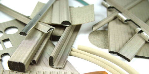
- Metal parts
- Partner
- MTC
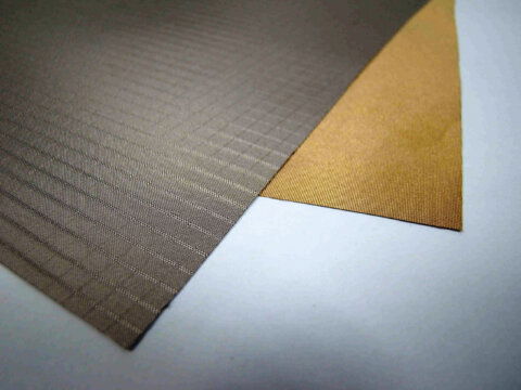
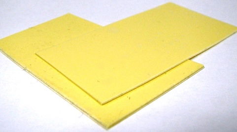
SMD contact pads are specialised surface-mount components designed to provide a reliable electrical grounding connection on printed circuit boards. They are used where a PCB must contact a chassis, lid, second board, cable shield, or other conductive element. Each pad combines a silicone-based core with a conductive outer layer to form a compressible spring-like contact that can be soldered directly onto the PCB. Type S versions use a conductive silicone core with a tin-plated copper foil base, while Type W versions use a silicone rubber core coated in a conductive film with tin or optional gold plating. Both versions are available in multiple sizes and are supplied on tape-and-reel for automated SMT assembly. These pads help maintain low impedance at high frequencies while also absorbing mechanical tolerances between mating surfaces. Once soldered in place during standard reflow assembly, they provide a durable grounding interface that withstands vibration, repeated compression, and demanding temperature conditions.
Range features
A high level overview of what this range offers
- Low contact resistance – Provides a low-impedance grounding path for EMI suppression and high-frequency stability.
- High heat tolerance – Supports lead-free reflow soldering and operates across a wide temperature range from –40 °C to +150 °C.
- Spring-like compliance – The flexible silicone core compresses to maintain reliable contact and absorb mechanical tolerances.
- Strong solder adhesion – Designed for secure SMT attachment and long-term stability under shock and vibration.
- Abrasion-resistant surface – Conductive outer materials are built to withstand repeated contact cycles.
- Efficient SMT assembly – Supplied on tape-and-reel for standard pick-and-place manufacturing.
- Optional gold plating – Type W versions are available with gold plating for improved corrosion resistance.
- RoHS & REACH compliant – Built from materials that meet common environmental compliance requirements.
What’s in this range?
All the variants in the range and a comparison of what they offer
| Specification | Type S (silicone paste) | Type W (conductive film) |
|---|---|---|
Core material | Conductive silicone rubber core | Silicone rubber core (with Ni/C filler) |
Outer conductive layer | Conductive silicone paste (silver-filled) | Conductive solderable film on all sides |
Solderable plating | Tin-plated copper foil base (Sn) | Tin (Sn) or Gold (Au) plating available |
Colour (appearance) | Beige | Silver |
Electrical contact resistance (max) | 0.9 Ω (under various stress tests) | 0.1 Ω (under various stress tests) |
Adhesion strength (min) | 19.6 N | 7.8 N |
Compression recovery | ≥ 95% height recovery after 20% compression (aging test) | ≥ 95% height recovery after 20% compression (aging test) |
Hardness | 65 ± 8 Shore A | 65 ± 8 Shore A |
Flammability rating | UL94 V-1 equivalent | UL94 V-0 equivalent |
Operating temperature range | –40 °C to +150 °C | –40 °C to +150 °C |
Standard width options | 2.0 mm (fixed for all Type S sizes) | 2.0 mm up to 10.0 mm |
Standard height range | 0.8 mm to 2.5 mm | 0.7 mm to 12.0 mm |
Standard length range | 1.0 mm to 1.8 mm | 1.0 mm to 8.4 mm |
Environmental compliance | RoHS & REACH compliant | RoHS & REACH compliant |
FAQs
for Surface mount device contact pads
SMD contact pads perform a similar grounding function to spring fingers or grounding clips, but they use a flexible conductive elastomer soldered directly onto the PCB. Instead of relying on moving metal parts, they provide compliance through their silicone structure, which can improve durability in high-vibration or high-temperature conditions. They also offer a broader contact area and precise placement during standard SMT assembly.
Type S pads use a conductive silicone core with a conductive silicone paste coating and a tin-plated copper foil base. Type W pads use a silicone rubber core with an outer conductive film and are available with tin or optional gold plating. Type S focuses on stronger post-solder adhesion, while Type W offers lower electrical resistance and improved corrosion-resistance options.
These pads are mounted using the normal SMT process. They are supplied in tape-and-reel format for pick-and-place assembly and are soldered during reflow onto the PCB land pattern. No special fixtures are typically required, so they integrate into standard electronics manufacturing workflows.
SMD contact pads are designed to compress under force and then recover close to their original height. A typical working compression is around 20% of pad height, and in some cases up to about 30% may be possible. Testing indicates at least 95% height recovery after 20% compression and aging, helping maintain stable long-term contact pressure.
Yes. The silicone-based construction supports operation from –40 °C to +150 °C and can withstand short-term lead-free reflow temperatures of around 240 °C during assembly. The materials are also designed for durability under humidity, thermal shock, and repeated compression. Type W is additionally available with gold plating for enhanced corrosion resistance.
The PCB should provide solder pad areas slightly larger than the contact pad footprint to support reliable soldering. It is also important to position the pad where the mating surface will compress it directly and to design the assembly so compression stays within the recommended range, typically around 10–30% of pad height. Nearby components should not interfere with pad movement or contact.
Yes. Type S pads are available in multiple sizes with a fixed width of 2.0 mm, heights from about 0.8 mm to 2.5 mm, and lengths from 1.0 mm to 1.8 mm. Type W pads cover a broader size range, with widths from about 2.0 mm to 10.0 mm, heights from 0.7 mm to 12.0 mm, and lengths up to 8.4 mm. This allows designers to choose a size based on the gap, alignment, and compression needs of the application.
In most applications, SMD contact pads are maintenance-free once soldered in place and are intended to last for the lifetime of the device. As long as recommended compression limits and environmental conditions are respected, they should not require replacement. If a product is frequently serviced or disassembled, periodic inspection for damage or contamination may still be advisable.