FB2M5LVR 650 nm 10-250 MBd 50 m LC POF Transceiver
- Technology
- Optical transceivers
- Partner
- Firecomms
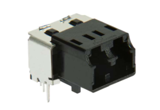
The FB2M5LVR LC POF transceiver is designed for engineers developing industrial, robotic, medical and transport data systems. Its integrated transmitter and receiver support Fast Ethernet, EtherCAT, Sercos III and proprietary links operating from 10 to 250 Mbps. A specified distance of 50 metres is supported at 250 Mbps with 0.5 NA step-index POF, while point-to-point Ethernet links can reach 80 metres at 125 Mbps depending on the installation. The electrical interface can be connected to LVDS, LVPECL and CML devices, including compatible PHYs, FPGAs and ASICs. A click-lock LC connection provides positive plug retention for installations exposed to vibration or mechanical shock. The transceiver operates from a nominal 3.3 V supply across a temperature range of −40 °C to +85 °C. Independent transmitter and receiver sleep functions reduce typical combined standby current to 27 µA when data and optical signals are absent.
Range features
A high level overview of what this range offers
- 650 nm RCLED transmitter: Supports red-light communication over plastic optical fibre.
- 10 to 250 Mbps data range: Covers Fast Ethernet, industrial Ethernet and proprietary data links.
- 50 metre link at 250 Mbps: Supports distributed equipment layouts using 0.5 NA step-index POF.
- LC click-lock connection: Helps retain the optical plug in vibration and shock environments.
- IEC 61754-20-compatible housing: Provides a defined LC interconnect format.
- LVDS, LVPECL and CML interfacing: Allows integration with suitable PHY, FPGA and ASIC devices.
- Integrated RCLED driver and PIN receiver: Reduces the number of external optical components required.
- 100 Ω receiver termination: Simplifies differential receiver connection and impedance matching.
- Signal-detect output: Enables the host circuit to monitor the presence of an optical input.
- Independent automatic sleep modes: Reduce typical combined standby current to 27 µA.
- −40 °C to +85 °C operation: Supports industrial equipment exposed to wide ambient temperatures.
- LED Class 1 and RoHS compliance: Supports defined eye-safety and restricted-substance requirements.
Downloads
for FB2M5LVR 650 nm 10-250 MBd 50 m LC POF Transceiver
What’s in this range?
All the variants in the range and a comparison of what they offer
Specifications
| Category | Parameter | Symbol / standard | Minimum | Typical | Maximum / level | Unit / condition |
|---|---|---|---|---|---|---|
General | Optical interconnect | IEC 61754-20 | — | — | Compliant | LC click-lock housing |
General | POF cable option | — | — | — | 2.2 | mm, black |
General | Data rate | — | 10 | — | 250 | Mbps |
General | Link distance | — | — | 50 | — | m at 250 Mbps with 0.5 NA step-index POF |
General | Extended point-to-point distance | — | — | — | 80 | m at 125 Mbps, installation-dependent |
General | Electrical interface types | — | — | — | LVDS, LVPECL, CML | Differential interface |
General | DC supply voltage | Vcc | 3.0 | 3.3 | 3.6 | V |
General | Operating temperature | Top | −40 | — | +85 | °C |
General | General dimensional tolerance | — | — | ±0.2 | — | mm |
Transmitter | Operating current consumption | Icc | — | 37 | 52 | mA |
Transmitter | Sleep-state current consumption | Isleep | — | 20 | 40 | µA |
Transmitter | Data input capacitance | CIN | — | — | 5 | pF |
Transmitter | Single-ended input resistance | RIN | — | 5 | — | kΩ |
Transmitter | Input common-mode range | VIN-BIAS | GND + 0.8 | — | Vcc − 0.8 | V |
Transmitter | Input voltage swing | VIN-SWING | 100 | — | 1,200 | mV |
Transmitter | Differential swing required for wake-up | Wake-up input | 50 | — | — | mV |
Transmitter | Wake-up delay | — | — | 5 | 80 | µs |
Transmitter | Optical power-off delay | — | 0.02 | — | 20 | µs |
Transmitter | Peak wavelength | λpeak | 640 | 660 | 670 | nm |
Transmitter | Spectral bandwidth, FWHM | Δλ | — | 23 | 30 | nm |
Transmitter | Average optical power | P | −10 | — | −2.0 | dBm |
Transmitter | Rise time, 20% to 80% | tR | — | 2.0 | 2.8 | ns |
Transmitter | Fall time, 80% to 20% | tF | 0.3 | — | 0.6 | ns |
Transmitter | Optical modulation amplitude | OMA | 160 | 590 | 1,250 | µW |
Transmitter | Total jitter | — | — | — | 1.6 | ns |
Receiver | Operating current consumption | Icc | 18 | 22 | 30 | mA |
Receiver | Sleep-state current consumption | Isleep | 2 | 7 | 15 | µA |
Receiver | Differential output impedance | — | — | 100 | — | Ω between RD+ and RD− |
Receiver | Output common-mode voltage | Vcm | 1.2 | 1.25 | 1.3 | V |
Receiver | Differential output voltage swing | — | 650 | 800 | 950 | mV |
Receiver | Receivable average optical power sensitivity | — | — | — | −24 | dBm |
Receiver | Maximum allowed average optical power | — | — | — | 0 | dBm |
Receiver | Rise time, 10% to 90% | — | — | 1.0 | 2.5 | ns |
Receiver | Fall time, 90% to 10% | — | — | 1.0 | 2.0 | ns |
Receiver | Wake-up time from sleep | — | — | 10 | 100 | µs |
Absolute rating | Storage temperature | Tstg | −40 | — | +85 | °C |
Absolute rating | Supply voltage | VR | −0.5 | — | 3.6 | V |
Absolute rating | Receiver optical overload | POL | — | — | 0 | dBm |
Assembly | Soldering temperature | Tsld | — | — | +260 | °C for 10 seconds, once only, at least 2.2 mm from the lead root |
Assembly | Reflow soldering | — | — | — | Not suitable | Infrared or vapour-phase reflow |
Compliance | Moisture sensitivity level | J-STD-020E | — | — | MSL 2a | Four-week floor life |
Compliance | Restriction of hazardous substances | Directive 2011/65/EU | — | — | Certified compliant | RoHS |
Compliance | Eye safety | IEC 60825-1 | — | — | LED Class 1 | — |
Electrical and optical characteristics are validated across −40 °C to +85 °C and a supply range of 3.0 to 3.6 V. Maximum-rate testing uses a 250 Mbps PRBS7 pattern unless another condition is stated. Transmitter optical power is characterised through 0.5 metres of 1 mm-diameter, 0.5 NA POF, while receiver measurements use at least 0.5 metres of the same fibre type.
Pin configuration
| Pin | Function | Symbol |
|---|---|---|
1 | Transmitter EMI shield | GND |
2 | Transmitter signal input, negative | TD− |
3 | Transmitter signal input, positive | TD+ |
4 | Transmitter ground | GND |
5 | Transmitter 3.3 V power input | Vcc |
6 | Transmitter ground | GND |
7 | Receiver 3.3 V power input | Vcc |
8 | Receiver ground | GND |
9 | Signal-detect output | SD |
10 | Receiver data output, negative | RD− |
11 | Receiver data output, positive | RD+ |
12 | Receiver EMI shield | GND |
Pins 1 and 12 should be connected to the PCB signal-ground plane. Both transmitter ground pins must also be connected because they are not joined internally. Follow the dimensional drawing and PCB footprint when defining the board layout, and do not place conductive traces beneath the electrically conductive housing’s seating surfaces.
Packaging information
| Packaging parameter | Value |
|---|---|
Components per tube | 25 |
Tube length | 450 mm |
Tube width | 34.9 mm |
Tube height | 19.4 mm |
Tubes per moisture-barrier bag | 10 |
Bags per inner carton | 1 |
Inner-carton length | 588 mm |
Inner-carton width | 147 mm |
Inner-carton height | 82 mm |
Complete inner-carton weight | 1.95 kg |
Components per inner carton | 250 |
Inner cartons per outer carton | 4 |
Outer-carton length | 600 mm |
Outer-carton width | 310 mm |
Outer-carton height | 195 mm |
Complete outer-carton weight | 8.10 kg |
Components per outer carton | 1,000 |
FAQs
for FB2M5LVR 650 nm 10-250 MBd 50 m LC POF Transceiver
At 250 Mbps, the specified reference distance is 50 metres using 0.5 NA step-index POF. At 125 Mbps Ethernet, a point-to-point link can reach 80 metres depending on the installation conditions. The optical figures provide a 14 dB starting budget between the minimum transmit power of −10 dBm and the receiver sensitivity of −24 dBm, before allowances for connectors, fibre attenuation, ageing and temperature. The strongest transmit level is −2 dBm, while the maximum receiver input is 0 dBm, leaving 2 dB before overload on a very short idealised link. Final reach should be checked against the actual cable, connector losses, bends, contamination and required design margin.
The FB2M5LVR handles the physical optical signal rather than implementing a particular network protocol or encoding method. A 100 Mbps Fast Ethernet application using 4B/5B encoding produces a 125 MBd optical symbol rate. An FPGA link carrying 200 Mbps with 8B/10B encoding produces a 250 MBd symbol rate because the encoding adds two transmitted bits for every eight payload bits. This distinction is important when comparing the payload requirement with the maximum signal rate seen by the transceiver. The selected PHY or FPGA must generate the required encoding, idle sequence and clock-recovery behaviour.
The electrical data paths are differential and can be connected to LVDS, CML or LVPECL devices through AC-coupled interface circuits. The receiver provides a typical 1.25 V common-mode level, an 800 mV differential swing and an internal 100 Ω differential termination. An LVDS interface normally operates at a 1.25 V common-mode level, while the CML side is typically biased to 1.5 V and the LVPECL side requires a termination network that establishes 2 V. Coupling capacitors of 100 nF are specified for high-speed operation from approximately 100 to 250 Mbps. Lower data rates may require larger capacitors, and the termination fitted inside the connected PHY, FPGA or ASIC must be checked before finalising the circuit.
The transmitter and receiver enter their sleep states independently. The transmitter sleeps when no data or toning signal is present, while the receiver sleeps when no optical input is detected. Typical sleep currents are 20 µA for the transmitter and 7 µA for the receiver, giving a combined typical value of 27 µA; the combined maximum is 55 µA. Transmitter wake-up takes 5 µs typically and up to 80 µs, with at least 50 mV differential input swing required to trigger wake-up, while receiver wake-up takes 10 µs typically and up to 100 µs. Designs requiring immediate response or continuous link supervision should account for these delays and maintain a suitable idle or toning pattern where necessary.
Correct grounding is required to control crosstalk, external interference and ESD exposure. EMI shield pins 1 and 12 should connect directly to the PCB signal-ground plane, and both transmitter ground pins, 4 and 6, must be connected because they are not internally linked. Differential data tracks should use controlled impedance and matched routing, while power-line capacitors should be positioned close to the relevant supply pins. The housing uses electrically conductive fibre-filled plastic, so conductive PCB traces should not pass beneath its defined seating surfaces. The mechanical footprint should be applied with its stated ±0.2 mm general tolerance to avoid electrical or mechanical conflicts.
The transceiver is not suitable for infrared or vapour-phase reflow soldering. The permitted soldering limit is 260 °C for 10 seconds on one occasion, with heat applied at least 2.2 mm from the lead root, and non-halogenated water-soluble flux is recommended. The optical dust plug should remain fitted during soldering, washing and drying, while suitable alcohol-based cleaning agents may be used; acetone, ethyl acetate and phenol-based products are not permitted. The component is rated MSL 2a, allowing 672 hours or four weeks below 30 °C and 60% relative humidity after opening. An unopened moisture-barrier bag has a 24-month shelf life below 40 °C and 90% relative humidity, while longer opened storage requires a dry cabinet below 10% relative humidity.
The transceiver is intended for systems that need a compact LC plastic-optical-fibre link with differential electrical signalling. Suitable applications include industrial networking, robotic connections, medical data systems and transport-system buses, with Fast Ethernet, EtherCAT, Sercos III and proprietary links identified as possible uses. Selection should take account of the 3.0 to 3.6 V supply, 10 to 250 Mbps signal range, optical budget and −40 °C to +85 °C operating range. It should be paired with a compatible PHY, FPGA or ASIC because protocol handling and encoding are not performed by the optical device. The through-hole soldering process, PCB keepout requirements and LC cable construction should also be considered before the board layout is released.