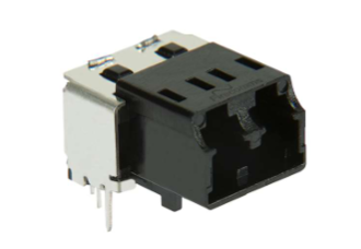
FB01GKAR 650 nm 1 Gbps 40 m OptoLock® POF Transceiver
- Technology
- Optical transceivers
- Partner
- Firecomms
The FB01GKAR combines an optical transmitter and receiver in a compact assembly for point-to-point Ethernet links in home and office data communication equipment. Its plugless OptoLock® port accepts bare 2.2 mm jacketed plastic optical fibre, eliminating the need for a separate optical plug at the transceiver. When paired with the KD1053 PHY IC, it supports 1 Gbps multilevel encoded operation and 100 Mbps Ethernet. Specified link lengths are up to 40 m at 1 Gbps and 100 m at 100 Mbps over step-index POF, with achievable distance depending on cable termination and installation conditions. Integrated lensed optics support coupling to 1 mm core, 0.5 NA POF, while the RSSI output indicates the average optical power reaching the receiver. The integrated transmitter uses a visible-red RCLED, and the receiver provides a low-current sleep state with defined optical sleep and wake thresholds. The transceiver operates from a nominal 3.3 V supply across an ambient air temperature range of -20 °C to +60 °C. PCB integration requires suitable grounding, thermal dissipation, supply filtering and controlled-impedance differential routing.
Range features
A high level overview of what this range offers
- Plugless OptoLock® termination: Accepts 2.2 mm jacketed bare POF without requiring a separate optical plug.
- Dual data-rate operation: Supports 1 Gbps and 100 Mbps modes when used with the KD1053 PHY IC.
- Defined POF link lengths: Enables links up to 40 m at 1 Gbps or 100 m at 100 Mbps, subject to termination and installation conditions.
- Integrated optical assembly: Combines a visible-red RCLED transmitter and PIN receiver in one compact transceiver.
- Lensed optical interface: Supports direct coupling to 1 mm core, 0.5 NA plastic optical fibre.
- RSSI monitoring output: Indicates average optical power at the receiver for link-health monitoring.
- Low-current receiver sleep state: Draws between 3.75 µA and 12.2 µA while asleep.
- Extended operating range: Operates at ambient air temperatures from -20 °C to +60 °C.
- Regulatory characteristics: Complies with RoHS requirements and the IEC 60825-1 LED Class 1 eye-safety classification.
- Integrated shielding: Supports EMI, EMC and ESD control when the shield and ground pins are connected as specified.
Downloads
for FB01GKAR 650 nm 1 Gbps 40 m OptoLock® POF Transceiver
What’s in this range?
All the variants in the range and a comparison of what they offer
Specifications
| Category | Parameter | Symbol | Value or range | Unit or condition |
|---|---|---|---|---|
General | Part number | FB01GKAR | Gigabit OptoLock® transceiver | |
General | Product option | Black | For 2.2 mm jacketed POF | |
General | Optical connection | Plugless bare-fibre termination | OptoLock® interface | |
General | POF characteristics | 1 mm core, 0.5 NA | Step-index POF under stated test conditions | |
Application | Typical application | Home or office data communications | Point-to-point link | |
Link | Maximum distance at 1 Gbps | Up to 40 m | Step-index POF; installation-dependent | |
Link | Maximum distance at 100 Mbps | Up to 100 m | Step-index POF; installation-dependent | |
Interface | 100 Mbps mode | 100 Mbps | IEEE 802.3 Ethernet | |
Interface | 1 Gbps mode | 1 Gbps | IEEE 802.3-bv multilevel encoded signal | |
Interface | PHY pairing | KD1053 | Required for 1 Gbps operation | |
Electrical | DC supply voltage | Vcc | 3.13 / 3.3 / 3.47 V | Minimum / typical / maximum |
Temperature | Operating air temperature | Top | -20 to +60 °C | Operating range |
Temperature | Storage temperature | Tstg | -40 to +85 °C | Storage range |
Temperature | EMI shield temperature | Maximum +85 °C | During operation | |
Mechanical | General dimensional tolerance | ±0.2 mm | Unless otherwise specified | |
Transmitter | Operating current | Icc | 61 / 71 / 75.5 mA | Minimum / typical / maximum |
Transmitter | Data rate, Gigabit mode | 1 Gbps | Multilevel encoded operation | |
Transmitter | Data rate, 100 Mbps mode | 100 Mbps | Ethernet operation | |
Transmitter | Optical source | Visible-red 650 nm RCLED | Integrated driver IC | |
Transmitter | Peak wavelength | λpeak | 660 nm typical | Defined optical test conditions |
Transmitter | Spectral bandwidth, FWHM | Δλ | 23 nm typical; 30 nm maximum | Defined optical test conditions |
Transmitter | Average optical power | P | -5 / -2.5 / -1.5 dBm | Minimum / typical / maximum |
Transmitter | Optical rise time, 20% to 80% | tR | 1.76 ns typical | Defined test conditions |
Transmitter | Optical fall time, 80% to 20% | tF | 1.83 ns typical | Defined test conditions |
Transmitter | Single-ended input impedance to ground | ZIN,SE | 46 / 50 / 54 Ω | Minimum / typical / maximum |
Transmitter | Single-ended input capacitance | CIN,TX+/- | 1.90 pF minimum; 2.33 pF typical | Per input |
Receiver | Operating current | Icc | 25.5 / 39 / 46 mA | Minimum / typical / maximum |
Receiver | Sleep-state current | Is | 3.75 / 7 / 12.2 µA | Minimum / typical / maximum |
Receiver | Input AOP for reliable link establishment | -16 to 0 dBm | Multilevel encoded operation | |
Receiver | Average optical power to enter sleep | PSL | -36 dBm typical | Sleep threshold |
Receiver | Average optical power to wake from sleep | PWU | -30 dBm typical | Wake threshold |
Receiver | Differential output voltage swing | VOUT,DIFF | 190 to 323 mV peak-to-peak | Minimum to maximum |
Receiver | Differential output impedance | ZDiff-Out | 100 Ω typical | Differential output |
Receiver | Common-mode output voltage | VOUT,CM | 0.6 / 0.96 / 1.12 V | Minimum / typical / maximum |
Receiver | RSSI output responsivity | IRSSI/PIN | 0.52 A/W typical | Average optical power monitoring |
Receiver | RSSI output current | IRSSI | 300 µA maximum | RSSI output |
Receiver | RSSI voltage compliance | VRSSI | 0.3 to 2.7 V | Operating range |
Receiver | Wake-up time | ton-wake | 24 µs typical | After AOP exceeds PWU |
Absolute rating | Supply voltage | VR | -0.5 to 4.5 V | Absolute maximum rating |
Absolute rating | Transmitter input voltage | Vin (Tx+/-) | -0.3 V to Vcc + 0.3 V | Absolute maximum rating |
Assembly | Soldering temperature | Tsld | Maximum +260 °C for 10 seconds | Once, at least 2.2 mm from the lead root |
Assembly | Reflow soldering | Not suitable | Includes infrared and vapour-phase reflow | |
Compliance | Moisture sensitivity level | MSL | 2a | J-STD-020; four-week floor life |
Compliance | Hazardous substances | RoHS | Directive 2011/65/EU | Includes Amendment 2015/863 |
Compliance | Eye safety | LED Class 1 | IEC 60825-1 | |
Storage | Unopened moisture-barrier bag life | 24 months | Below 40 °C and 90% RH | |
Storage | Open-bag floor life | 672 hours | Below 30 °C and 60% RH | |
Storage | Dry-cabinet condition | Below 10% RH | Alternative storage after opening |
Electrical and optical characteristics are validated across the -20 °C to +60 °C operating range and a 3.3 V ±5% supply range. Transmitter optical power is measured through 0.5 m of professionally terminated 1 mm core, 0.5 NA POF, while receiver input measurements use a minimum fibre length of 1 m. Maximum link length varies with the data rate, cable termination and installation conditions. Footprint and placement dimensions must be taken directly from the mechanical drawing in the datasheet.
Pin assignment
| Pin | Function | Symbol |
|---|---|---|
1 | Transmitter EMI shield | GND |
2 | Transmitter ground | GND |
3 | Transmitter ground | GND |
4 | Positive signal input | TD+ |
5 | Negative signal input | TD− |
6 | Transmitter 3.3 V DC power input | Vcc |
7 | Receiver 3.3 V DC power input | Vcc |
8 | Receiver ground | GND |
9 | Received signal strength indicator | RSSI |
10 | Positive data output | RD+ |
11 | Negative data output | RD− |
12 | Receiver EMI shield | GND |
Pins 1 and 12 must connect to the PCB signal-ground plane, while transmitter ground pins 2 and 3 require a full ground plane for heat transfer. Isolate each Vcc supply using a ferrite bead rated at 600 Ω at 100 MHz with a DCR below 200 mΩ, and position local power capacitors close to the DC input pins. Route TD+/TD− and RD+/RD− as controlled-impedance, high-speed differential pairs.
Packing information
| Packing parameter | Value |
|---|---|
Components per tube | 25 |
Tube dimensions | 430 × 31 × 20 mm |
Tubes per bag | 10 |
Bags per inner carton | 1 |
Inner carton dimensions | 588 × 147 × 84 mm |
Complete inner carton weight | 1.80 kg |
Components per inner carton | 250 |
Inner cartons per outer carton | 4 |
Outer carton dimensions | 600 × 310 × 195 mm |
Complete outer carton weight | 7.53 kg |
Components per outer carton | 1,000 |
FAQs
for FB01GKAR 650 nm 1 Gbps 40 m OptoLock® POF Transceiver
The KD1053 PHY IC is required for 1 Gbps operation, and it also supports the 100 Mbps mode. Gigabit transmission relies on the prescribed multilevel encoded signal used for IEEE 802.3-bv over POF, so the transceiver should not be paired with an arbitrary Ethernet PHY. The 100 Mbps mode follows IEEE 802.3 Ethernet while retaining the same optical transceiver assembly. TD+ and TD− feed the transmitter, while RD+ and RD− carry the receiver output, and these differential paths require controlled-impedance routing. In practice, the PHY, transceiver, PCB layout and selected operating mode should be validated as one complete link.
The specified design targets are up to 40 m at 1 Gbps and up to 100 m at 100 Mbps over step-index POF. The optical interface is intended for 2.2 mm jacketed cable, with optical characterisation based on 1 mm core, 0.5 NA POF. Transmitter power testing uses 0.5 m of professionally terminated fibre, while receiver testing uses a minimum fibre length of 1 m. Actual maximum distance can change with the data rate, fibre condition, bend routing, termination quality and installation environment. Link-budget and system testing should therefore be completed using the intended production cable and termination process.
The transceiver should be powered from 3.3 V, with an operating range of 3.13 to 3.47 V. Transmitter current is 61 to 75.5 mA and receiver current is 25.5 to 46 mA, so their maximum values sum to 121.5 mA before allowing for the PHY and design margin. The supply should be isolated with a ferrite bead rated at 600 Ω at 100 MHz and below 200 mΩ DCR, with local power capacitors placed close to the DC pins. EMI shield pins 1 and 12 must connect to the signal-ground plane, while transmitter ground pins 2 and 3 need a full ground plane for heat transfer. Keep the device away from hot components, provide enclosure airflow and ensure that the EMI shield remains below 85 °C.
The RSSI output represents the average optical power reaching the receiver and can be used to monitor link condition. Its typical responsivity is 0.52 A/W, with a maximum output current of 300 µA and a compliance range of 0.3 to 2.7 V. The receiver enters sleep at an average optical power of -36 dBm and wakes when the level reaches -30 dBm. These thresholds create 6 dB of optical hysteresis, while the typical output wake-up time is 24 µs after the wake threshold is crossed. This allows the controller or PHY to distinguish between an inactive optical path and a signal level suitable for restoring receiver operation.
The PCB should treat TD+/TD− and RD+/RD− as high-speed differential paths and route them with consistent impedance and minimal discontinuities. Each transmitter input has a typical single-ended impedance of 50 Ω, with limits of 46 to 54 Ω, and a typical input capacitance of 2.33 pF. The receiver presents a 100 Ω differential output impedance and a differential swing between 190 and 323 mV peak-to-peak. Its common-mode output voltage ranges from 0.6 to 1.12 V, with a typical value of 0.96 V. These characteristics should be checked against the PHY input requirements, PCB stack-up and termination strategy before layout approval.
The transceiver is not suitable for infrared or vapour-phase reflow soldering, so it requires a compatible lead-soldering process. The absolute soldering limit is 260 °C for 10 seconds on one occasion, with the heat applied at least 2.2 mm from the lead root. It is classified as MSL 2a under J-STD-020, providing a floor life of 672 hours, or four weeks, below 30 °C and 60% relative humidity after the bag is opened. An unopened moisture-barrier bag has a stated shelf life of 24 months below 40 °C and 90% relative humidity. Assembly should use static-control procedures, non-halogenated water-soluble flux and compatible alcohol-based cleaning agents, with the dust plug kept in place during soldering, washing and drying.
The 650 nm designation describes the visible-red RCLED technology used by the product, while the electrical and optical characteristics give a typical measured peak wavelength of 660 nm. The stated spectral bandwidth is 23 nm typical and 30 nm maximum, so the emitted energy occupies a wavelength range rather than a single exact line. Average optical output power is specified from -5 to -1.5 dBm, with a typical value of -2.5 dBm under the defined fibre-coupling conditions. The emitter is classified as LED Class 1 in accordance with IEC 60825-1. Optical power-budget calculations should use the specified power and wavelength characteristics rather than assuming that the emission peak is fixed at exactly 650 nm.