CT-1250TSR-MB4L-A 1310 nm FP 10 km 1.25 Gb/s SFF Transceiver
- Technology
- Optical transceivers
- Partner
- Coretek
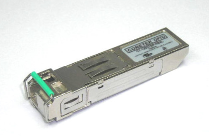
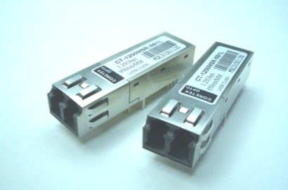
The CT-1250TSR-MB4L-A is a board-mounted optical transceiver for bidirectional serial communication over single-mode fibre. It combines a 1310 nm FP transmitter and optical receiver in an MSA-compatible 2×5 SFF package with a duplex LC receptacle. The module supports 1.25 Gb/s NRZ operation and link distances up to 10 km. Intended applications include Gigabit Ethernet, 1.06 Gb/s Fibre Channel, high-speed backplane interconnects and switched backbones. Its 3.3 V electrical interface provides AC-coupled differential data paths, TTL transmitter disable and TTL signal detection. An ambient operating range of −40 to +85 °C supports equipment installed beyond standard indoor temperature conditions. Separate transmitter and receiver supply connections, a defined pin allocation and board-integration guidance simplify planned PCB implementation.
Range features
A high level overview of what this range offers
- 1.25 Gb/s NRZ operation: Supports IEEE 802.3z Gigabit Ethernet physical links.
- 1.06 Gb/s Fibre Channel compatibility: Allows use with corresponding ANSI Fibre Channel applications.
- 1310 nm FP laser with 10 km rating: Provides an intermediate-reach link over single-mode fibre.
- MSA 2×5 SFF footprint: Supports integration into fixed, board-mounted optical interfaces.
- Duplex LC receptacle: Provides separate transmit and receive fibre connections in a compact interface.
- 3.3 V AC/AC differential interface: Connects to low-voltage serial data circuitry through AC-coupled paths.
- TTL transmitter disable and signal detect: Provides host control and optical link-status monitoring.
- −40 to +85 °C ambient range: Supports equipment intended for extended-temperature environments.
- Class 1 operation under EN 60825-1: Supports laser-safety integration requirements.
- RoHS-compliant, lead-free construction: Supports restricted-substance requirements for electronic equipment.
Downloads
for CT-1250TSR-MB4L-A 1310 nm FP 10 km 1.25 Gb/s SFF Transceiver
What’s in this range?
All the variants in the range and a comparison of what they offer
Specifications
| Category | Parameter | Minimum | Typical / stated | Maximum | Unit | Conditions / notes |
|---|---|---|---|---|---|---|
General | Data rate | — | 1.25 | — | Gb/s | NRZ signalling |
General | Fibre Channel rate | — | 1.06 | — | Gb/s | ANSI Fibre Channel applications |
General | Link distance | — | 10 | — | km | Single-mode fibre |
General | Nominal wavelength | — | 1310 | — | nm | FP laser diode |
General | Fibre type | — | Single-mode | — | — | Optical power measured using 9/125 µm fibre |
General | Optical connector | — | Duplex LC | — | — | Separate transmit and receive paths |
General | Form factor | — | 2×5 SFF | — | — | MSA footprint |
General | Electrical data interface | — | AC/AC differential | — | — | Transmit and receive paths |
General | Signal-detect output | — | TTL | — | — | High level indicates a received optical signal |
General | Ethernet compatibility | — | IEEE 802.3z | — | — | 1.25 Gb/s |
General | Fibre Channel compatibility | — | ANSI Fibre Channel | — | — | 1.06 Gb/s |
General | Optical safety | — | Class 1 | — | — | EN 60825-1 |
General | Reliability characterisation | — | Telcordia GR-468-CORE | — | — | Characteristics evaluated in accordance with the specification |
General | EMC design intent | — | FCC Class B | — | — | EN 55022 and CISPR 22 identified for equipment-level consideration |
Absolute maximum | Storage temperature, TS | −40 | — | 85 | °C | — |
Absolute maximum | Supply voltage, VCC | 0 | — | 6 | V | Not an operating range |
Absolute maximum | Lead soldering temperature | — | — | 260 | °C | Maximum 10 seconds on the lead |
Absolute maximum | Data input voltage | 0 | — | VCC | V | — |
Operating condition | Ambient temperature, TA | −40 | — | 85 | °C | — |
Operating condition | Supply voltage, VCC | 3.1 | 3.3 nominal | 3.5 | V | — |
Operating condition | Data input voltage swing, VID | 400 | — | 1660 | mV | Differential input |
Electrical | Transmitter supply current, ICCT | — | — | 140 | mA | — |
Electrical | Transmit-disable input low, VIL | — | — | 0.8 | V | TTL input |
Electrical | Transmit-disable input high, VIH | VCC−1.3 | — | VCC | V | TTL input |
Electrical | Receiver supply current, ICCR | — | — | 100 | mA | — |
Electrical | Receiver differential output, VOD | 0.4 | — | 1.3 | V | — |
Electrical | Signal-detect output low, VOL | — | — | 0.8 | V | TTL output |
Electrical | Signal-detect output high, VOH | 2.0 | — | — | V | TTL output |
Transmitter optical | Average optical output power, PO | −9.5 | — | −3 | dBm | Coupled into 9/125 µm single-mode fibre |
Transmitter optical | Extinction ratio, ER | 9 | — | — | dB | — |
Transmitter optical | Centre wavelength | 1275 | 1310 nominal | 1355 | nm | Wavelength conditions reference IEEE 802.3z and FC-PI |
Transmitter optical | RMS spectral width | — | — | 3 | nm | — |
Transmitter optical | Relative intensity noise, RIN | — | — | −120 | dB/Hz | — |
Transmitter optical | Optical rise time, 20–80% | — | — | 260 | ps | — |
Transmitter optical | Optical fall time, 20–80% | — | — | 260 | ps | — |
Transmitter optical | Output eye | — | IEEE 802.3z/D5.0 | — | — | — |
Receiver optical | Maximum input optical power, Pmax | −3 | — | — | dBm | Measured with a 2⁷−1 PRBS at BER below 10⁻¹² |
Receiver optical | Receiver sensitivity, Pmin | — | — | −21 | dBm | Measured with a 2⁷−1 PRBS at BER below 10⁻¹² |
Receiver optical | Operating wavelength | 1100 | — | 1600 | nm | — |
Receiver optical | Optical return loss, ORL | 12 | — | — | dB | — |
Receiver electrical | 3 dB upper cut-off frequency | — | — | 1500 | MHz | — |
Receiver status | Loss-of-signal asserted threshold, PD | — | — | −21 | dBm | Transition-note mapping in the source is unclear |
Receiver status | Loss-of-signal deasserted threshold, PA | −35 | — | — | dBm | Transition-note mapping in the source is unclear |
Pin allocation
| Pin | Symbol | Function |
|---|---|---|
1 | VEER | Receiver signal ground |
2 | VCCR | Receiver power supply |
3 | SD | TTL signal-detect output; high indicates a received optical signal |
4 | RD− | Receiver inverted differential data output |
5 | RD+ | Receiver non-inverted differential data output |
6 | VCCT | Transmitter power supply |
7 | VEET | Transmitter signal ground |
8 | TXDIS | Transmitter disable input |
9 | TD+ | Transmitter non-inverted differential data input |
10 | TD− | Transmitter inverted differential data input |
The mounting posts provide mechanical attachment to the circuit board. They should not be connected to circuit ground, although connection to chassis ground is permitted.
FAQs
for CT-1250TSR-MB4L-A 1310 nm FP 10 km 1.25 Gb/s SFF Transceiver
Yes, provided the complete channel loss remains within the available optical budget. Using the minimum launch power of −9.5 dBm and the receiver sensitivity limit of −21 dBm gives a worst-case nominal budget of 11.5 dB under the stated test conditions. That budget must cover fibre attenuation, connectors, splices, temperature effects, ageing and the required engineering margin. At the opposite end, the maximum launch power is −3 dBm and the receiver maximum-input specification is also −3 dBm, so a short, low-loss path can operate close to the upper receiver limit. Check both total channel loss and receiver overload when validating the link.
The host requires a 3.3 V rail maintained between 3.1 and 3.5 V, AC-coupled differential data paths and TTL-compatible control and status connections. The transmitter accepts a differential input swing from 400 to 1660 mV, while the receiver differential output is specified from 0.4 to 1.3 V. TXDIS provides transmitter control, and SD goes high when an optical signal is detected. Separate transmitter and receiver supply and ground pins allow local filtering around each section. Match the host transceiver’s coupling and voltage requirements, route both differential pairs symmetrically and verify the TTL thresholds before releasing the PCB.
Yes, it is specified for ambient operation from −40 to +85 °C, with storage over the same temperature range. This supports equipment exposed to wider temperatures than standard indoor networking hardware, provided the module’s local ambient remains within the specified limits. The transmitter and receiver can draw up to 140 mA and 100 mA respectively, so enclosure temperature and local heat generation still require consideration. No separate case-temperature or junction-temperature limit is stated, making board-level and enclosure-level thermal testing important. Verify start-up behaviour, optical margin and signal integrity at both temperature extremes.
Yes, the optical and electrical characteristics are intended for IEEE 802.3z Gigabit Ethernet at 1.25 Gb/s and ANSI Fibre Channel at 1.06 Gb/s. The transmitter uses NRZ signalling and its output eye is specified against IEEE 802.3z/D5.0, while the wavelength conditions reference both IEEE 802.3z and FC-PI. This does not make the module a protocol converter; framing, coding, clock recovery and link management remain functions of the host electronics. The same module can therefore serve either application when the host PHY and timing are configured for the relevant standard. Confirm the complete electrical interface and protocol implementation separately.
Design the 3.3 V rail for at least the sum of the maximum transmitter and receiver currents, which is 240 mA. At the maximum allowed supply voltage of 3.5 V, this equates to 0.84 W before adding margin for tolerances, transient demand and losses in the local filtering network. The rail must remain within 3.1 to 3.5 V during start-up and steady operation. Separate VCCT and VCCR pins should be locally decoupled and filtered rather than supplied through long shared traces. This arrangement can help limit interaction between transmitter switching activity and the receiver signal path.
The PCB must accommodate an MSA 2×5 SFF footprint, ten signal and power pins, mechanical mounting posts and the front-facing duplex LC receptacle. The pin allocation separates transmitter and receiver data, power and grounds, while TXDIS and SD provide control and link-status functions. The mounting posts are intended for mechanical retention and should not be connected to circuit ground, although they may be connected to chassis ground. Dimensioned mechanical and host-board drawings are provided in the datasheet for direct use during PCB and enclosure design. Complete connector-access, insertion-clearance and chassis-ground reviews before finalising the layout.
The module is designed for Class 1 laser operation under EN 60825-1 and is identified as RoHS-compliant and lead-free. Its EMC design targets FCC Class B limits and identifies CENELEC EN 55022 and CISPR 22 as equipment-level requirements, but final compliance depends on the complete host system. Enclosure apertures, PCB routing, grounding, power filtering and cable configuration can alter emissions and immunity. The transceiver characteristics also reference Telcordia GR-468-CORE evaluation practices. Treat these points as component-level design inputs and complete the required system-level safety, EMC and materials assessments for the finished equipment.