FB2M5KRR 650 nm 10-250 Mbps 50 m OptoLock® POF Transceiver
- Technology
- Optical transceivers
- Partner
- Firecomms
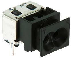
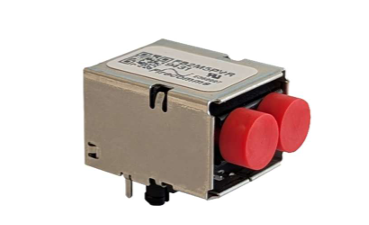
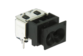
The FB2M5KRR is a compact, plugless POF transceiver for bidirectional links over 2.2 mm jacketed plastic optical fibre. It handles NRZ symbol rates from 10 to 250 Mbps and supports link distances up to 50 m over step-index POF at 250 Mbps, subject to installation and operating conditions. The device is designed for industrial and robotic communication links, including 100BASE-FX, EtherCAT, Sercos III and 200 Mbps 8B/10B serial connections. Its differential electrical interface can be adapted to LVDS, LVPECL and CML ports on PHY, FPGA and ASIC devices. An RSSI output provides an analogue indication related to average received optical power for link monitoring. Automatic transmitter and receiver sleep functions reduce typical combined sleep current to 27 µA when activity is absent. Operation across −40 °C to +85 °C supports deployment in industrial equipment.
Range features
A high level overview of what this range offers
- Plugless connection for 2.2 mm jacketed POF – Allows bare-fibre termination without a separate optical plug.
- 10 to 250 Mbps NRZ operation – Supports Fast Ethernet, industrial Ethernet and proprietary serial links.
- 50 m link distance at 250 Mbps – Accommodates distributed industrial and robotic communication paths, subject to installation conditions.
- 650 nm RCLED optical transmitter – Provides a red optical source suited to 0.5 NA plastic optical fibre.
- RSSI current output – Enables analogue monitoring of average received optical power.
- Automatic transmitter and receiver sleep modes – Reduce typical combined sleep current to 27 µA during inactivity.
- LVDS, LVPECL and CML compatibility – Supports connection to a range of PHY, FPGA and ASIC interfaces.
- Internally terminated receiver output – Provides 100 Ω differential termination between RD+ and RD−.
- −40 °C to +85 °C operation – Supports equipment used across an industrial temperature range.
- Integrated shielding and differential signalling – Helps manage crosstalk and electromagnetic interference when correctly grounded and laid out.
- RSSI, transmitter and receiver in one housing – Combines optical conversion and link monitoring in a single through-hole component.
- RoHS compliance and LED Class 1 classification – Supports relevant material and optical safety requirements.
Downloads
for FB2M5KRR 650 nm 10-250 Mbps 50 m OptoLock® POF Transceiver
What’s in this range?
All the variants in the range and a comparison of what they offer
Unless otherwise indicated, electrical and optical characteristics apply across −40 °C to +85 °C with a 3.0 V to 3.6 V supply. Maximum-rate characterisation used a 250 Mbps PRBS7 pattern, while optical measurements used 0.5 m of 1 mm core, 0.5 NA plastic optical fibre.
Specifications
| Category | Specification | Minimum | Typical / nominal | Maximum or limit | Unit / notes |
|---|---|---|---|---|---|
General | Data rate | 10 | — | 250 | Mbps; maximum NRZ symbol rate |
General | Nominal optical technology | — | 650 nm RCLED | — | Integrated CMOS driver |
General | Fibre connection | — | Bare 2.2 mm jacketed POF | — | Plugless OptoLock® port |
General | Optical test fibre | — | 1 mm core, 0.5 NA step-index POF | — | Used for optical characterisation |
General | Link distance | — | — | 50 | m at 250 Mbps; installation dependent |
General | Supported link examples | — | 100BASE-FX, EtherCAT, Sercos III and 200 Mbps 8B/10B serial links | — | Protocol processing is external |
General | Operating supply voltage | 3.0 | 3.3 | 3.6 | V |
General | Operating temperature | −40 | — | +85 | °C |
General | Typical combined sleep current | — | 27 | — | µA; transmitter and receiver combined |
Absolute maximum | Supply voltage | −0.5 | — | 3.6 | V |
Absolute maximum | Storage temperature | −40 | — | +85 | °C |
Absolute maximum | Soldering temperature | — | — | +260 | °C for 10 seconds, once only, at least 2.2 mm from the lead root |
Transmitter | Operating current | — | 37 | 52 | mA |
Transmitter | Sleep-state current | — | 20 | 40 | µA |
Transmitter | Data input capacitance | — | 5 | — | pF |
Transmitter | Single-ended input resistance | — | 5 | — | kΩ |
Transmitter | Input common-mode range | GND + 0.8 | — | VCC − 0.8 | V |
Transmitter | Input voltage swing | 100 | — | 1,200 | mV |
Transmitter | Differential swing required for wake-up | 50 | — | — | mV |
Transmitter | Wake-up delay | — | 5 | 80 | µs |
Transmitter | Optical power-off delay | 0.02 | — | 20 | µs |
Transmitter | Peak wavelength | 640 | 660 | 670 | nm |
Transmitter | Spectral bandwidth, FWHM | — | 23 | 30 | nm |
Transmitter | Average optical power | −10 | — | −2.0 | dBm |
Transmitter | Optical rise time, 20–80% | — | 2.0 | 2.8 | ns |
Transmitter | Optical fall time, 20–80% | 0.3 | — | 0.6 | ns |
Transmitter | Optical modulation amplitude | 160 | 590 | 1,250 | µW |
Transmitter | Total jitter | — | — | 1.6 | ns |
Receiver | Operating current | 18 | 22 | 30 | mA |
Receiver | Sleep-state current | 2 | 7 | 15 | µA |
Receiver | Differential output impedance | — | 100 | — | Ω between RD+ and RD− |
Receiver | Output common-mode voltage | 1.15 | 1.25 | 1.35 | V |
Receiver | Single-ended peak-to-peak output swing | 325 | 400 | 500 | mV |
Receiver | Differential output swing | 650 | 800 | 1,000 | mV |
Receiver | Optical sensitivity | — | — | −24 | dBm |
Receiver | Maximum permitted optical input | — | — | −2 | dBm |
Receiver | Rise time, 10–90% | — | 0.4 | 1 | ns |
Receiver | Fall time, 90–10% | — | 0.4 | 1 | ns |
Receiver | Optical power for entry into sleep | −40 | −31 | — | dBm |
Receiver | Optical power for wake from sleep | −28 | — | −26 | dBm |
Receiver | Sleep-state delay | — | 2 | — | s |
Receiver | Wake time from sleep | — | 100 | — | µs |
Receiver | Jitter | — | — | 1.5 | ns with an ideal input signal |
Receiver | RSSI voltage range | 0 | — | VCC − 1.5 | V |
Receiver | RSSI output responsivity | — | 0.16 | — | A/W |
Mechanical | General dimensional tolerance | — | ±0.2 | — | mm |
Housing | Colour | — | Black | — | Standard housing option |
Pin assignment
| Pin | Function | Symbol |
|---|---|---|
1 | Transmitter EMI shield | SHIELD |
2 | Negative transmitter signal input | TD− |
3 | Positive transmitter signal input | TD+ |
4 | Transmitter ground | GND |
5 | Transmitter 3.3 V power input | VCC |
6 | Transmitter ground | GND |
7 | Receiver 3.3 V power input | VCC |
8 | Receiver ground | GND |
9 | Received signal strength indicator | RSSI |
10 | Negative receiver data output | RD− |
11 | Positive receiver data output | RD+ |
12 | Receiver EMI shield | SHIELD |
The shield pins should be connected to the signal ground plane. Both transmitter ground pins must be connected because they are not internally joined.
Regulatory compliance
| Parameter | Symbol | Standard | Level |
|---|---|---|---|
Moisture sensitivity | MSL | J-STD-020 | Level 2a, four-week floor life |
Restriction of hazardous substances | RoHS | Directive 2011/65/EU | Certified compliant |
Eye safety | — | IEC 60825-1 | LED Class 1 |
Packing information
| Packing parameter | Value |
|---|---|
Components per tube | 25 |
Tube length | 430 mm |
Tube width | 31 mm |
Tube height | 20 mm |
Tubes per moisture barrier bag | 10 |
Bags per inner carton | 1 |
Inner carton length | 588 mm |
Inner carton width | 147 mm |
Inner carton height | 84 mm |
Complete inner carton weight | 1.80 kg |
Components per inner carton | 250 |
Inner cartons per outer carton | 4 |
Outer carton length | 600 mm |
Outer carton width | 310 mm |
Outer carton height | 195 mm |
Complete outer carton weight | 7.53 kg |
Components per outer carton | 1,000 |
FAQs
for FB2M5KRR 650 nm 10-250 Mbps 50 m OptoLock® POF Transceiver
The FB2M5KRR supports NRZ data from 10 to 250 Mbps, allowing it to be used for Fast Ethernet, industrial Ethernet and proprietary serial links within that symbol-rate range. A 100 Mbps Ethernet connection using 4B/5B encoding operates at 125 MBd, while a 200 Mbps 8B/10B link operates at 250 MBd and therefore reaches the maximum specified rate. Suitable application examples include 100BASE-FX, EtherCAT, Sercos III and compatible FPGA or ASIC serial ports. Protocol processing remains external, as the transceiver converts the differential electrical stream to and from the optical link rather than implementing the communication protocol.
The electrical data paths should normally be AC-coupled, with the interface network selected for the common-mode voltage of the connected device. The receiver operates with a nominal 1.25 V common-mode output, while the illustrated CML and LVPECL interfaces use common-mode levels of 1.5 V and 2 V respectively. RD+ and RD− are internally terminated with 100 Ω, but TD+ and TD− require an external 100 Ω differential termination. Coupling capacitors of 100 nF are used for high-speed operation, although a larger value may be needed at lower data rates. The final network should be checked against the termination and biasing requirements of the chosen PHY, FPGA or ASIC.
The 50 m rating applies to step-index plastic optical fibre at 250 Mbps and is dependent on the completed installation. Optical characterisation uses 1 mm core, 0.5 NA POF, with transmitter output specified from −10 to −2 dBm and receiver sensitivity specified at −24 dBm. The receiver permits a maximum optical input of −2 dBm, defining the upper end of its accepted optical range. Fibre attenuation, bends, termination quality, contamination and operating temperature can all affect the available margin in practice. The intended cable route and termination process should therefore be validated at the required data rate and across the equipment’s operating conditions.
The RSSI pin provides a current proportional to the average optical power reaching the receiver. Connecting a suitable resistor between RSSI and ground converts this current into an analogue voltage that can be read by an ADC or monitoring circuit. RSSI output responsivity is typically 0.16 A/W, and the permitted RSSI voltage range extends from 0 V to VCC minus 1.5 V. With the nominal 3.3 V supply, this gives an upper electrical range of 1.8 V. Link-health thresholds should be established in the finished system because the measured value will also reflect fibre loss, connector condition, component variation and the selected load resistor.
The transmitter and receiver independently enter low-current states when electrical or optical activity is absent. Typical sleep currents are 20 µA for the transmitter and 7 µA for the receiver, producing the stated combined typical value of 27 µA. The receiver has a typical two-second delay before entering sleep and a typical 100 µs wake time, with an optical wake threshold between −28 and −26 dBm. The transmitter requires at least 50 mV differential input swing to initiate wake-up, with a typical delay of 5 µs and an 80 µs maximum. Designs using intermittent traffic should account for these wake intervals when setting packet timing, link supervision and retry behaviour.
The data lines should be routed as impedance-controlled differential pairs with short, balanced paths and a continuous low-inductance ground plane. RD+ and RD− already have 100 Ω differential termination, while the transmitter input requires an external 100 Ω resistor between TD+ and TD−. The EMI shield pins and all ground pins should be connected to the signal ground plane, and supply bypass capacitors should be placed close to the relevant power pins. Pins 6 and 7 require non-circular top and bottom solder pads measuring 1.2 mm by 1.5 mm, although their plated through-holes remain circular. The mechanical layout has a general dimensional tolerance of ±0.2 mm and should be implemented from the controlled footprint drawing.
The component is not suitable for infrared or vapour-phase reflow soldering. The absolute soldering limit is +260 °C for 10 seconds, once only, with the heat applied at least 2.2 mm from the lead root. The dust plug should remain fitted during soldering, washing and drying, while non-halogenated water-soluble fluxes and compatible alcohol-based cleaners may be used; acetone, ethyl acetate and phenol-based products are not permitted. The device is classified as MSL 2a and has a 672-hour floor life below 30 °C and 60% relative humidity after the moisture barrier bag is opened. Alternatively, opened components can be kept in a dry cabinet below 10% relative humidity.
Normal operation is specified from −40 °C to +85 °C with a supply between 3.0 V and 3.6 V, centred on a nominal 3.3 V rail. The absolute supply range of −0.5 V to 3.6 V is a damage limit and should not be treated as an operating range. The optical source is classified as LED Class 1 under IEC 60825-1, while material compliance covers RoHS Directive 2011/65/EU. Moisture handling follows J-STD-020 at MSL 2a. These component-level classifications support equipment selection, but electrical safety, EMC, ESD and regulatory compliance must still be evaluated for the finished system.