FE50MSNR 650 nm DC-50 MBd 50 m SMI POF Non-Inverting Transceiver
- Technology
- Optical transceivers
- Partner
- Firecomms
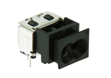
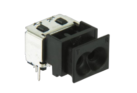
The FE50MSNR is a board-mounted SMI POF transceiver with separate transmitting and receiving channels for duplex communication. Its transmitter combines a visible red 650 nm RCLED with an integrated driver, while the receiver uses a dual-differential photodiode front end and a push-pull TTL/LVTTL-compatible CMOS output. Both channels are non-inverting, retaining the electrical logic polarity across the optical link. The device handles DC levels, PWM signals and digital data at rates up to 50 MBd, with a maximum stated frequency of 25 MHz. Applications include instrument control, industrial automation, serial communication, voltage isolation and equipment operating in areas with electrical interference. It can provide the optical physical layer for RS232, RS485, Modbus or PROFIBUS systems when the surrounding interface circuitry and protocol timing are suitable. Support for 3.3 V and 5 V rails simplifies integration with different logic families, while the −40 °C to +85 °C ambient range supports industrial installations. The latched SMI connection, conductive plastic body and metal shield provide mechanical retention and support static-discharge and electromagnetic-compatibility requirements.
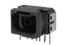
The FE50MSNR integrates a visible-red optical transmitter and a non-inverting receiver in a board-mounted, latched SMI package. Separate Tx and Rx channels enable full-duplex communication over duplex step-index plastic optical fibre. The DC-capable signal path supports static levels, PWM, burst traffic and continuous digital data, while the conductive housing and metal shield help address installations exposed to static discharge and electrical interference.
Range features
A high level overview of what this range offers
- 650 nm RCLED transmitter – Provides a visible red optical signal for step-index POF links.
- DC to 50 MBd operation – Supports static levels, PWM, burst traffic and continuous digital data.
- Up to 50 m link distance – Accommodates machine, cabinet and instrument links when installation loss remains within budget.
- Non-inverting transmitter and receiver – Retains the original logic polarity across the optical connection.
- Separate Tx and Rx channels – Enables full-duplex communication over duplex POF cable.
- 3.3 V or 5 V operation – Supports integration with TTL and LVTTL logic environments.
- Push-pull CMOS receiver output – Provides defined high and low output states within the specified loading limits.
- −40 °C to +85 °C operating range – Supports industrial ambient conditions.
- Tx pulse-width distortion of −3 ns to +3 ns – Supports timing-sensitive and burst-mode signalling.
- Latched SMI interface – Provides a retained plug connection for duplex POF cabling.
- Conductive housing and metal shield – Supports static-discharge control and operation in electrically noisy environments.
- LED Class 1 and RoHS compliance – Addresses the listed eye-safety and restricted-substance requirements.
Downloads
for FE50MSNR 650 nm DC-50 MBd 50 m SMI POF Non-Inverting Transceiver
What’s in this range?
All the variants in the range and a comparison of what they offer
Core specifications
| Specification | Value |
|---|---|
Part number | FE50MSNR |
Product type | Duplex SMI plastic optical fibre transceiver |
Optical source | 650 nm RCLED with integrated driver |
Transmitter logic | Non-inverting |
Receiver logic | Non-inverting |
Fibre type | Step-index plastic optical fibre |
Link distance | Up to 50 m, depending on installation conditions |
Data rate | DC to 50 MBd |
Maximum stated frequency | 25 MHz |
Minimum unit interval | 20 ns |
Supply options | 3.3 V or 5 V; Tx and Rx may use separate rails, although a common rail is recommended |
Logic interface | TTL input and push-pull TTL/LVTTL-compatible CMOS output |
Operating temperature | −40 °C to +85 °C ambient |
Connection | Latched SMI duplex connector |
Variant comparison
| Specification | FE50MSNR | FE50MSIR |
|---|---|---|
Product identifier | FE50MSNR | FE50MSIR |
Transmitter polarity | Non-inverting | Non-inverting |
Receiver polarity | Non-inverting | Inverting |
Data-rate range | DC to 50 MBd | DC to 50 MBd |
Connector type | SMI | SMI |
Transceiver pin assignment
| Pin | Function | Symbol |
|---|---|---|
1 | Transmitter EMI shield | GND |
2 | TTL data input | Vin |
3 | Transmitter ground | GND |
4 | Transmitter ground | GND |
5 | Transmitter supply, 5 V or 3.3 V | VCC |
6 | Transmitter supply, 5 V or 3.3 V | VCC |
7 | Receiver supply, 5 V or 3.3 V | VCC |
8 | Receiver supply, 5 V or 3.3 V | VCC |
9 | Receiver ground | GND |
10 | Receiver data output | Vo |
11 | No connection | NC |
12 | Receiver EMI shield | GND |
EMI shield pins 1 and 12 should be connected to the PCB signal-ground plane to limit Tx-to-Rx crosstalk and improve shielding against external EMI, EMC and ESD. A common supply rail is recommended for the transmitter and receiver, with 3.3 V preferred where compatible to reduce power consumption. The mechanical drawing specifies a general dimensional tolerance of ±0.2 mm. Pins 6 and 7 require non-circular top and bottom solder pads measuring 1.2 mm by 1.5 mm, with standard plated circular through-holes.
Regulatory compliance
| Parameter | Symbol | Standard | Level or status |
|---|---|---|---|
Human Body Model contact ESD | HBM | JEDEC JS-001 | Level 2, 2 kV to less than 4 kV |
Moisture sensitivity | MSL | J-STD-020E | Level 2a, four-week floor life |
Restriction of hazardous substances | RoHS | Directive 2011/65/EU, including Amendment 2015/863 | Certified compliant |
Eye safety | Not applicable | IEC 60825-1 | LED Class 1 |
Absolute maximum ratings
| Parameter | Symbol | Minimum | Maximum | Unit |
|---|---|---|---|---|
Storage temperature | Tstg | −40 | +85 | °C |
Operating temperature | Top | −40 | +85 | °C |
Soldering temperature | Tsld | Not specified | +260 | °C |
Tx and Rx supply voltage | VCC | −0.5 | +7 | V |
Tx data-input voltage | VIN | −0.5 | VCC + 0.5 | V |
Rx output current | IO | −16 | +16 | mA |
The +260 °C soldering limit applies for ten seconds, once only, at least 2.2 mm from the lead root. Functional operation above the 5.5 V recommended operating limit is not implied by the +7 V absolute maximum supply rating. VIN must not exceed VCC during power-up because this can place the transmitter driver in an uncontrolled logic state. The dust plug must not be exposed to temperatures above 110 °C during soldering.
Transmitter electrical and optical characteristics
| Parameter | Symbol | Minimum | Typical | Maximum | Unit | Condition |
|---|---|---|---|---|---|---|
Supply current | ICC | Not specified | 16.5 at 3.3 V; 17.5 at 5 V | 27 | mA | T1 |
Input voltage, low | VIL | −0.3 | Not specified | 0.8 | V | T1 |
Input voltage, high | VIH | 2 | Not specified | VCC + 0.25 | V | T1 |
Data-input capacitance | Cin | Not specified | Not specified | 7 | pF | Not specified |
Data-input resistance | Rin | 10 | Not specified | Not specified | MΩ | Not specified |
Peak optical output power | PHigh | −9 | Not specified | −1 | dBm | T1, T2 |
Emission wavelength, centroid | λc | 640 | 650 | 680 | nm | T4 |
Spectral width, RMS | λRMS | Not specified | Not specified | 30 | nm | T5 |
Optical rise time, 20% to 80% | tr | Not specified | 1.6 | 5 | ns | T1 |
Optical fall time, 80% to 20% | tf | Not specified | 1.3 | 2 | ns | T1 |
Propagation delay, low to high | tPropDly-LH | 13 | 22 | 30 | ns | T1 |
Propagation delay, high to low | tPropDly-HL | 13 | 22 | 30 | ns | T1 |
Transmitter pulse-width distortion | PWD | −3 | Not specified | +3 | ns | T1, T4 |
Power-up wake delay | tpower-on | Not specified | 20 | Not specified | µs | T6 |
Transmitter test conditions: T1 covers validation across −40 °C to +85 °C and both 3.3 V and 5 V supplies at ±5%; typical figures use 25 °C, a 3.3 V supply and 50 Mbit/s PRBS data. T2 uses peak optical power coupled into 0.5 m of 1 mm diameter, 0.5 NA POF and measured with a large-area detector; for 50% duty-cycle data, peak power is twice the average power. T4 defines the wavelength centroid in accordance with EIA/TIA FOTP-127/6.1. T5 defines RMS spectral width in accordance with EIA/TIA FOTP-127/6.3. T6 measures the interval from valid power-up to valid data output with 50% duty-cycle input data.
Receiver electrical and optical characteristics
| Parameter | Symbol | Minimum | Typical | Maximum | Unit | Condition |
|---|---|---|---|---|---|---|
Supply current | ICC | Not specified | 20 | 25 | mA | R2, R3, R4 |
Power-up wake delay | tpower-on | Not specified | 40 | Not specified | µs | R1 |
High-level output voltage | VOH | VCC − 0.05 | Not specified | VCC | V | IOH maximum 40 µA, R2 |
Low-level output voltage | VOL | 0 | Not specified | 0.05 | V | IOL maximum 1.6 mA, R2 |
Optical power high | PH | −22 | Not specified | −1 | dBm | R2, R3 |
Optical power low | PL | Not specified | Not specified | −40 | dBm | R2, R3 |
Data rate | Not applicable | DC | Not specified | 50 | MBd | Minimum UI 20 ns; maximum frequency 25 MHz |
Output rise time, 10% to 90% | tr | Not specified | Not specified | 6 | ns | R2, R3, R4 |
Output fall time, 90% to 10% | tf | Not specified | Not specified | 6 | ns | R2, R3, R4 |
PWD for PH range −20 to +2 dBm | PWD | −4 | Not specified | +4 | ns | R2, R3, R4, R5 |
PWD for PH range −20 to −22 dBm | PWD | −6 | Not specified | +6 | ns | R2, R3, R4, R5 |
First-to-third-pulse distortion | PWDinit | −7 | Not specified | +14 | ns | R2, R3, R4, R5, R6 |
Propagation delay, high to low | tPropDly-HL | Not specified | Not specified | 50 | ns | R2, R3, R4 |
Propagation delay, low to high | tPropDly-LH | Not specified | Not specified | 50 | ns | R2, R3, R4 |
Receiver test conditions: R1 measures the delay from VCC exceeding 2.75 V until the output responds correctly; the output remains in a high-impedance state before this point. R2 covers a 635 nm to 680 nm transmitter with 5 ns rise and fall times, operation from −40 °C to +85 °C and 3.3 V or 5 V supplies at ±5%; typical values apply at 25 °C. R3 uses the recommended transmitter signal. R4 uses a receiver load of 50 kΩ with 15 pF total capacitance. R5 characterises PWD with 50 MBd NRZ PRBS7 data at a bit error rate of 10⁻⁹ or lower. R6 uses a minimum optical input pulse width of 20 ns; longer pulses produce lower initial distortion, while rates below 1 MBd should be assessed using the initial PWD figures.
Packing information
| Packing parameter | Value |
|---|---|
Components per tube | 25 |
Tube length | 444 mm |
Tube width | 26 mm |
Tube height | 19.4 mm |
Tubes per moisture-barrier bag | 10 |
Bags per inner carton | 1 |
Inner-carton length | 588 mm |
Inner-carton width | 147 mm |
Inner-carton height | 84 mm |
Complete inner-carton weight | 1.80 kg |
Components per inner carton | 250 |
Inner cartons per outer carton | 4 |
Outer-carton length | 600 mm |
Outer-carton width | 310 mm |
Outer-carton height | 195 mm |
Complete outer-carton weight | 7.53 kg |
Components per outer carton | 1,000 |
FAQs
for FE50MSNR 650 nm DC-50 MBd 50 m SMI POF Non-Inverting Transceiver
Yes. Its signal path is specified from DC to 50 MBd, so it can convey static optical levels, low-frequency PWM and NRZ digital data without requiring a minimum transition rate. At the upper limit, the minimum unit interval is 20 ns and the stated maximum frequency is 25 MHz. The FE50MSNR can therefore provide an optical physical layer for systems based on RS232, RS485, Modbus or PROFIBUS, provided the external interface circuitry and protocol timing remain within the electrical and timing limits. For long idle periods or burst traffic, the initial receiver pulse-width distortion should be checked alongside the steady-state timing figures.
The FE50MSNR uses a non-inverting transmitter and non-inverting receiver, so a logic-high electrical input produces light and detected light produces a logic-high receiver output. The FE50MSIR has the same non-inverting transmitter but uses an inverting receiver, reversing the receive-output polarity. This distinction matters when replacing copper links, handling serial-interface idle states or connecting directly to programmable logic with a defined active level. During receiver power-up, the output remains in a high-impedance state and settles within 40 µs after VCC reaches the operating threshold. Variant selection should therefore consider both normal logic polarity and the equipment’s required start-up and fail-state behaviour.
Either rail can be used, with electrical performance validated at 3.3 V and 5 V supplies within ±5%. A 3.3 V rail is preferred where the connected logic permits it because the typical transmitter current is 16.5 mA at 3.3 V compared with 17.5 mA at 5 V. The transmitter and receiver may use separate rails, although operating both from the same supply is recommended. During start-up, VIN must not exceed VCC because the transmitter driver could otherwise enter an uncontrolled logic state. The +7 V value is an absolute maximum rating and must not be treated as an operating supply limit; normal operation above 5.5 V is not specified.
The 50 m figure should be treated as an installation-dependent link distance rather than an unconditional cable-length guarantee. Peak transmitter output is specified from −9 dBm to −1 dBm, while the receiver optical-high range extends from −22 dBm to −1 dBm. Comparing the minimum launch level with the minimum high-level threshold gives a simple 13 dB loss allowance before accounting for engineering margin. Fibre attenuation, connector losses, bending, contamination, temperature and ageing must all fit within the final optical budget. Optical figures are stated as peak values, so measurements taken as average power on 50% duty-cycle data will be approximately 3 dB lower and must be interpreted accordingly.
Allow for up to 30 ns of transmitter propagation delay and up to 50 ns of receiver propagation delay for either transition, giving as much as 80 ns of internal end-to-end delay before adding the installed link’s additional delay. At 50 MBd, one unit interval is 20 ns, so fixed latency may span several unit intervals even though it does not directly reduce the steady-state eye opening. Transmitter pulse-width distortion is limited to −3 ns to +3 ns, while receiver PWD is specified at up to ±4 ns or ±6 ns depending on received optical power. The first three received pulses can show −7 ns to +14 ns distortion. Burst protocols should therefore include enough preamble or timing tolerance for the initial pulses to settle.
Pins 1 and 12 are EMI shield connections and should be tied to the PCB signal-ground plane to reduce Tx-to-Rx crosstalk and improve shielding against external interference and ESD. The layout also requires particular attention around pins 6 and 7, where 1.2 mm by 1.5 mm oval solder-pad areas are specified on the top and bottom copper. The component is suitable for wave soldering but not for reflow soldering, and hand soldering is not recommended for production. The soldering limit is 260 °C for ten seconds, once only, at least 2.2 mm from the lead root. The dust plug may remain fitted during processing but must remain below 110 °C, and Moisture Sensitivity Level 2a handling controls apply.
The FE50MSNR is specified for −40 °C to +85 °C operation and carries IEC 60825-1 LED Class 1, RoHS and JEDEC Human Body Model Level 2 ratings. The HBM level of 2 kV to less than 4 kV is a component-handling rating and does not represent finished-equipment immunity to external ESD events. Likewise, the mention of medical control, patient safety and voltage isolation describes possible application areas rather than complete medical-equipment or functional-safety certification. Designers must still establish the required creepage, clearance, insulation, EMC and equipment-level safety performance. The optical link can support galvanic separation, but no system isolation-voltage rating is defined for the completed installation.