CT-1250TBP-JB4L-E 1490 nm DFB/1310 nm PIN 10 km 1.25 Gb/s SFP Bi-Di Transceiver w. DDMI
- Technology
- Optical transceivers
- Partner
- Coretek
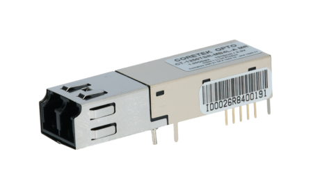
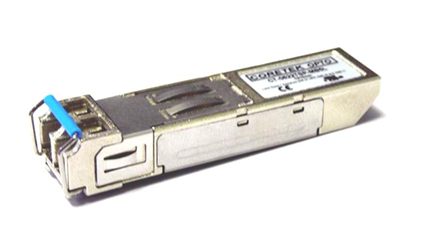
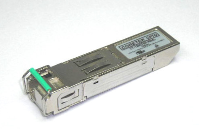
The CT-1250TBP-JB4L-E SFP Bi-Di transceiver is designed for 1.25 Gb/s single-fibre optical links, including 1000BASE-BX-OLT and Gigabit Ethernet connections. It uses a 1490 nm DFB laser for transmission and a 1310 nm PIN receiver, allowing both communication directions to share one 9/125 µm single-mode fibre strand. A single LC receptacle provides the optical connection, with a specified transmission distance of up to 10 km. The module operates from a nominal 3.3 V supply and supports case temperatures from −40 to +85 °C. An SFF-8472-compatible I²C interface provides digital diagnostic and serial identification functions for integration with host management systems. Typical applications include switched backbones, high-speed backplane interconnects and other 1.25 Gb/s optical connections requiring an SFP MSA interface.
Range features
A high level overview of what this range offers
- 1490 nm DFB transmitter and 1310 nm PIN receiver: Supports bidirectional communication over one single-mode fibre strand.
- 1.25 Gb/s NRZ data rate: Suits Gigabit Ethernet and IEEE 802.3ah optical links.
- 10 km specified reach: Supports intermediate-reach connections across campus, access and industrial networks.
- Single LC optical interface: Reduces the number of fibre strands required for a link.
- SFP MSA form factor: Supports integration into compatible pluggable host ports.
- 3.1 to 3.5 V operating supply: Aligns with standard 3.3 V SFP host power rails.
- SFF-8472 DDMI interface: Provides serial diagnostic and identification access over I²C.
- Defined optical limits: Delivers −9 to −3 dBm transmit output and receiver sensitivity of −20 dBm or lower for link-budget calculations.
- −40 to +85 °C case temperature range: Supports equipment exposed to extended operating temperatures.
- TX_DISABLE, TX_FAULT and RX_LOS signals: Provide host control, transmitter fault indication and optical signal-loss status.
- IEEE 802.3ah output-eye alignment: Supports integration into 1000BASE-BX10-D link designs.
- Class 1 laser and compliant construction: Addresses EN 60825-1 optical safety requirements and uses RoHS-compliant, lead-free materials.
Downloads
for CT-1250TBP-JB4L-E 1490 nm DFB/1310 nm PIN 10 km 1.25 Gb/s SFP Bi-Di Transceiver w. DDMI
What’s in this range?
All the variants in the range and a comparison of what they offer
Specifications
| Category | Parameter | Symbol | Requirement or range | Unit | Conditions or notes |
|---|---|---|---|---|---|
General | Product type | — | 1000BASE-BX-OLT SFP Bi-Di transceiver | — | Single-fibre optical interface |
General | Data rate | — | 1.25 | Gb/s | NRZ |
General | Transmission distance | — | Up to 10 | km | Single-mode fibre |
General | Fibre type | — | 9/125 | µm | Single-mode fibre |
General | Optical connector | — | Single LC | — | Bidirectional connection |
General | Transmit source | — | 1490 nm DFB laser | — | 1480 to 1500 nm operating range |
General | Receive detector | — | 1310 nm PIN | — | 1260 to 1360 nm operating range |
General | Nominal supply | Vcc | 3.3 | V | Operating range specified below |
General | Electrical interface | — | AC/AC differential | — | SFP host interface |
General | Signal-detect output | — | TTL | — | Receiver status output |
General | Digital diagnostics | — | SFF-8472 DDMI | — | I²C serial interface |
General | Host form-factor standard | — | SFP MSA | — | Small Form Factor Pluggable |
General | Ethernet alignment | — | IEEE 802.3ah 1000BASE-BX10-D | — | Output eye compliant with IEEE 802.3ah |
General | Optical safety | — | Laser Class 1, EN 60825-1 | — | Eye-safety design |
General | Materials | — | RoHS compliant and lead-free | — | — |
General | Reliability reference | — | Telcordia GR-468-CORE | — | Electro-optical characteristics |
General | EMC design intent | — | FCC Class B | — | Host equipment requires separate EMC verification |
Absolute maximum | Storage temperature | Ts | −40 to +85 | °C | — |
Absolute maximum | Supply voltage | Vcc | 0 to 6 | V | — |
Absolute maximum | Data input voltage | — | 0 to Vcc | V | — |
Absolute maximum | Supply current | Is | 300 maximum | mA | — |
Operating | Case operating temperature | Ta | −40 to +85 | °C | — |
Operating | Supply voltage | Vcc | 3.1 to 3.5 | V | — |
Operating | Data input voltage swing | Vid | 300 to 1860 | mV | — |
Electrical | Transmitter supply current | Icct | 200 maximum | mA | — |
Electrical | TX_DISABLE input, low | Vil | 0 to 0.8 | V | — |
Electrical | TX_DISABLE input, high | Vih | 2.0 to Vcc | V | High or open disables transmission |
Electrical | TX_FAULT output, low | Vol | 0 to 0.8 | V | — |
Electrical | TX_FAULT output, high | Voh | 2.0 to Vcc | V | — |
Electrical | Receiver supply current | Iccr | 100 maximum | mA | — |
Electrical | Receiver differential output | Vod | 0.4 to 1.3 | V | — |
Electrical | RX_LOS output, low | Vol | 0 to 0.8 | V | — |
Electrical | RX_LOS output, high | Voh | 2.0 to Vcc | V | — |
Electrical | MOD-DEF(1) and MOD-DEF(2), low | Vil | −0.6 to Vcc × 0.3 | V | — |
Electrical | MOD-DEF(1) and MOD-DEF(2), high | Vih | Vcc × 0.7 to Vcc + 0.5 | V | — |
Transmitter | Optical output power | Po | −9 to −3 | dBm | Average power coupled into 9/125 µm single-mode fibre |
Transmitter | Extinction ratio | ER | 6 minimum | dB | — |
Transmitter | Centre wavelength | λc | 1480 to 1500 | nm | 1490 nm typical |
Transmitter | Spectral width, RMS | Δλ | 0.4 maximum | nm | — |
Transmitter | Side-mode suppression ratio | SMSR | 30 minimum | dB | — |
Transmitter | Relative intensity noise | RIN | −120 maximum | dB/Hz | — |
Transmitter | Optical rise time, 20–80% | tr | 260 maximum | ps | — |
Transmitter | Optical fall time, 20–80% | tf | 260 maximum | ps | — |
Transmitter | Output eye | — | IEEE 802.3ah compliant | — | — |
Receiver | Maximum input optical power | Pmax | −3 | dBm | Receiver overload limit |
Receiver | Minimum input optical power | Pmin | ≤ −20 | dBm | Measured with 2⁷−1 PRBS at BER <10⁻¹² |
Receiver | Operating wavelength | λ | 1260 to 1360 | nm | 1310 nm typical |
Receiver | Optical return loss | ORL | 14 minimum | dB | — |
Receiver | LOS asserted threshold | Pa | −35 | dBm | — |
Receiver | LOS deasserted threshold | Pd | −19 | dBm | — |
Receiver | LOS hysteresis | Pd − Pa | 0.5 minimum | dB | — |
Timing | TX_DISABLE assert time | t_off | 10 maximum | µs | — |
Timing | TX_DISABLE negate time | t_on | 1 maximum | ms | — |
Timing | Initialisation and TX_FAULT reset | t_init | 300 maximum | ms | — |
Timing | Fault-to-TX_FAULT assertion | t_fault | 100 maximum | µs | — |
Timing | TX_DISABLE reset pulse | t_reset | 10 minimum | µs | — |
Timing | RX_LOS off-to-on transition | tA,RX_LOS | 100 maximum | µs | — |
Timing | RX_LOS on-to-off transition | tD,RX_LOS | 100 maximum | µs | — |
SFP Pin Assignment
| Pin | Symbol | Functional description |
|---|---|---|
1 | VeeT | Transmitter ground |
2 | TX Fault | Transmitter fault indication |
3 | TX Disable | Transmitter disable; high or open disables the module |
4 | MOD-DEF(2) | Two-wire serial identification interface |
5 | MOD-DEF(1) | Two-wire serial identification interface |
6 | MOD-DEF(0) | Grounded within the module |
7 | Rate Select | Not connected |
8 | LOS | Loss-of-signal indication |
9 | VeeR | Receiver ground |
10 | VeeR | Receiver ground |
11 | VeeR | Receiver ground |
12 | RD− | Inverted received-data output |
13 | RD+ | Received-data output |
14 | VeeR | Receiver ground |
15 | VccR | Receiver power |
16 | VccT | Transmitter power |
17 | VeeT | Transmitter ground |
18 | TD+ | Transmitter data input |
19 | TD− | Inverted transmitter data input |
20 | VeeT | Transmitter ground |
FAQs
for CT-1250TBP-JB4L-E 1490 nm DFB/1310 nm PIN 10 km 1.25 Gb/s SFP Bi-Di Transceiver w. DDMI
This is a single-fibre Bi-Di optic, so it must be paired with a device that transmits at 1310 nm and receives at 1490 nm. The CT-1250TBP-JB4L-E transmits nominally at 1490 nm and receives across 1260 to 1360 nm, with 1310 nm as the typical receive wavelength. Both ends must support 1.25 Gb/s NRZ operation and compatible 1000BASE-BX signalling. The far-end output power, receiver overload limit and sensitivity must also be checked, because complementary wavelengths alone do not guarantee link compatibility. The exact complementary part number is not defined, so pairing should be confirmed against the complete optical limits of the remote module.
A provisional 11 dB span can be inferred from the −9 dBm minimum transmit output and −20 dBm receiver sensitivity, but this is not a complete bidirectional link budget. The transmit output may range from −9 to −3 dBm, while the maximum receiver input is −3 dBm, so the fibre path must avoid both insufficient received power and overload on short, low-loss links. Each direction should be calculated using the transmitting module at one end and the receiver limits of the complementary module at the other. Fibre attenuation at both wavelengths, connectors, splices, contamination, ageing and an engineering margin must be included. Final acceptance should therefore use the optical limits of both installed transceivers rather than the nominal 10 km distance alone.
The host should provide a regulated 3.3 V rail that remains within 3.1 to 3.5 V at the module. Maximum transmitter and receiver supply currents are 200 mA and 100 mA respectively, so the slot power design should allow up to 300 mA with suitable board-level margin. The data input swing is 300 to 1860 mV, while the receiver differential output is 0.4 to 1.3 V and the data interface is AC-coupled. Separate VccT and VccR pins, together with their associated grounds, should follow the SFP pin allocation; Rate Select is not connected. Power filtering, sequencing and differential routing should follow the recommended host-interface arrangement and SFP MSA layout practices.
DDMI and serial identification are accessed through the SFF-8472-compatible I²C interface on MOD-DEF(1) and MOD-DEF(2), with MOD-DEF(0) grounded within the module. The individual DDMI measurement channels are not itemised, so host firmware should verify the implemented memory map rather than assume a particular set of monitored values. TX_DISABLE recognises 0 to 0.8 V as low and 2.0 V to Vcc as high; a high or open input disables transmission. TX_FAULT and RX_LOS use corresponding low and high output ranges, while initialisation may take up to 300 ms and fault or LOS transitions up to 100 µs. These timings should be incorporated into hot-swap logic, link bring-up delays and alarm filtering.
The specified case operating range is −40 to +85 °C, with the same limits applying to storage temperature. The supply must remain between 3.1 and 3.5 V throughout operation, and optical link margin should be verified at the temperature extremes rather than only at room temperature. The module is RoHS-compliant and lead-free, while its electro-optical characteristics are stated in relation to Telcordia GR-468-CORE. Its EMC design intent includes FCC Class B limits, but the complete host assembly still requires its own EMC verification. For sealed outdoor cabinets or dense chassis, the system design should also address airflow, condensation, connector cleanliness and local hot-spot temperature around the SFP cage.
The optical interface is aligned with IEEE 802.3ah 1000BASE-BX10-D, and the transmitter output eye is specified as compliant with IEEE 802.3ah. Mechanical and electrical host integration follows the SFP Multi-Source Agreement, while digital diagnostics use an SFF-8472-compatible interface. The laser is designed for Class 1 eye safety under EN 60825-1, and the construction is stated as RoHS-compliant and lead-free. The EMC design targets FCC Class B limits and references the CENELEC EN 55022 or CISPR 22 equipment environment. These module-level statements do not replace safety, EMC or regulatory testing of the finished host equipment.
The intended medium is 9/125 µm single-mode fibre connected through one LC interface, with a specified link distance of up to 10 km. The single-fibre WDM arrangement makes it suitable for Gigabit Ethernet links where fibre availability is limited or where one strand must carry both directions. Listed application areas include switched backbones and high-speed backplane interconnects, provided that the host supports the 1.25 Gb/s SFP electrical interface. It is not a direct replacement for a dual-LC duplex optic, a multimode transceiver or a module requiring a different line rate. Installation planning should include a complementary wavelength pair, clean optical connections and a verified loss budget for both transmission directions.