HVA Wideband Voltage Amplifier
- Technology
- Amplifiers
- Partner
- FEMTO Messtechnik
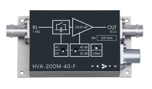
The HVA Series is a family of wideband voltage amplifiers for measuring and recording small, fast-changing voltage signals. It is designed for use ahead of oscilloscopes, transient recorders and other 50 Ω measurement equipment. Five variants cover upper cut-off frequencies of 10, 200 and 500 MHz. The 10 MHz pair offers switchable gains of 40 and 60 dB, while the 200 MHz pair provides 20 and 40 dB settings. The 500 MHz model uses a fixed gain of 20 dB and maintains true DC coupling for pulse and digital-signal measurements. Engineers can choose between 50 Ω bipolar inputs for impedance-matched, low-noise signal chains and 1 MΩ FET inputs where reduced source loading and low bias current are required.
Adjustable output offset assists with baseline alignment and preservation of the available output range. Typical uses include photomultiplier and microchannel-plate signal amplification, optical-receiver signal boosting and time-resolved pulse or transient measurements.
Range features
A high level overview of what this range offers
- 10, 200 and 500 MHz bandwidth options: Match the amplifier bandwidth to the signal without introducing unnecessary wideband noise.
- Gain settings from 20 to 60 dB: Support voltage gains from ×10 to ×1,000 for signals at different amplitude levels.
- 50 Ω bipolar input variants: Provide impedance matching and input voltage noise as low as 0.9 nV/√Hz.
- 1 MΩ FET input variants: Reduce loading on high-impedance sources and provide input bias currents down to 2 pA.
- True DC coupling throughout the range: Preserve pulse baselines, long transients and digital signal levels.
- Switchable AC/DC coupling on 10 and 200 MHz models: Reject low-frequency or DC components when required.
- Constant bandwidth between switchable gain settings: Maintain the amplifier’s time response when changing gain.
- Adjustable output offset: Position the baseline and manage the available output swing.
- 50 Ω output with short-circuit protection: Support direct connection to impedance-matched measuring instruments.
- BNC signal connections: Simplify integration with common laboratory and test equipment.
- ±0.2 dB gain accuracy: Provide predictable voltage scaling across all five variants.
Downloads
for HVA Wideband Voltage Amplifier
What’s in this range?
All the variants in the range and a comparison of what they offer
Range specifications
| Specification | Range details |
|---|---|
Product type | Wideband voltage amplifier |
Available models | HVA-10M-60-B, HVA-10M-60-F, HVA-200M-40-B, HVA-200M-40-F, HVA-500M-20-B |
Test conditions | ±15 V supply, 25 °C ambient temperature |
Upper cut-off frequencies | 10 MHz, 200 MHz or 500 MHz |
Lower cut-off frequency | DC on every model; switchable to 1 kHz on B-input 10 and 200 MHz models or 1 Hz on F-input 10 and 200 MHz models |
Gain options | 20, 40 or 60 dB; equivalent to ×10, ×100 or ×1,000 |
Gain accuracy | ±0.2 dB |
Input stage options | 50 Ω bipolar input or 1 MΩ FET input |
Input voltage noise | 0.9 to 5.5 nV/√Hz, depending on model and gain setting |
Input voltage drift | 1 to 10 µV/°C, depending on model |
Input voltage absolute maximum | ±5 V |
F-input transient rating | 200 V from a 200 pF source |
Output impedance | 50 Ω; a 50 Ω load is recommended |
Linear output voltage | ±3.5 V for 10 MHz models; ±1 V for 200 and 500 MHz models, measured with a 50 Ω load |
Maximum output current | 60 or 100 mA, depending on model |
Output offset adjustment | ±500 mV for 10 MHz models; ±100 mV for 200 and 500 MHz models |
Output protection | Short-circuit protected |
Supply voltage | ±15 V DC |
Recommended supply capability | Minimum ±150 mA |
Absolute maximum supply voltage | ±20 V |
Operating temperature | 0 to +60 °C |
Storage temperature | −40 to +100 °C |
Signal connectors | BNC input and BNC output |
Power connection | 3-pin fixed power socket; mating connector supplied |
Case weight | 200 g |
Case material | Nickel-plated AlMg4.5Mn |
Optional power supply | PS-15 |
Variant comparison
| Specification | HVA-10M-60-B | HVA-10M-60-F | HVA-200M-40-B | HVA-200M-40-F | HVA-500M-20-B |
|---|---|---|---|---|---|
Lower cut-off frequency | DC or 1 kHz | DC or 1 Hz | DC or 1 kHz | DC or 1 Hz | DC |
Upper cut-off frequency | 10 MHz | 10 MHz | 200 MHz | 200 MHz | 500 MHz ±10% |
Gain | 40 or 60 dB | 40 or 60 dB | 20 or 40 dB | 20 or 40 dB | 20 dB |
Rise/fall time, 10–90% | 35 ns | 35 ns | 1.8 ns | 1.8 ns | 750 ps |
Input impedance | 50 Ω in parallel with 12 pF | 1 MΩ in parallel with 15 pF | 50 Ω in parallel with 12 pF | 1 MΩ in parallel with 15 pF | 50 Ω in parallel with 3 pF |
Input voltage noise | 0.9 nV/√Hz at 60 dB; 1.8 nV/√Hz at 40 dB, measured at 2 MHz | 4.7 nV/√Hz at 2 MHz | 1.2 nV/√Hz at 40 dB; 3.5 nV/√Hz at 20 dB, measured at 50 MHz | 4.5 nV/√Hz at 40 dB; 5.5 nV/√Hz at 20 dB, measured at 50 MHz | 3.0 nV/√Hz at 200 MHz |
Integrated input noise, peak-to-peak | 20 µV at 60 dB; 50 µV at 40 dB | 100 µV | 150 µV at 40 dB; 400 µV at 20 dB | 450 µV at 40 dB; 600 µV at 20 dB | 0.5 mV |
Input bias current | 18 µA | 2 pA | 20 µA | 10 pA | 15 µA typical |
Input offset voltage | 500 µV typical | 250 µV maximum | 500 µV typical | 500 µV typical | 1 mV typical |
Input voltage drift | 1 µV/°C | 2 µV/°C | 1 µV/°C | 5 µV/°C | 10 µV/°C |
Linear output voltage into 50 Ω | ±3.5 V | ±3.5 V | ±1 V | ±1 V | ±1 V |
Maximum output current | 100 mA | 100 mA | 60 mA | 60 mA | 100 mA |
Output offset trimmer range | ±500 mV | ±500 mV | ±100 mV | ±100 mV | ±100 mV |
Slew rate into 50 Ω | 500 V/µs | 500 V/µs | 500 V/µs at 20 dB; 1,000 V/µs at 40 dB | 600 V/µs at 20 dB; 1,100 V/µs at 40 dB | 2,600 V/µs |
Typical supply current | ±70 mA | ±70 mA | ±70 mA | ±70 mA | ±40 mA |
Additional transient input rating | — | 200 V from a 200 pF source | — | 200 V from a 200 pF source | — |
FAQs
for HVA Wideband Voltage Amplifier
Select the narrowest model that still passes the highest frequency and edge rate the measurement must preserve. The 10 MHz variants have a 35 ns rise/fall time and suit slower pulses, detector outputs and transient measurements that do not require hundreds of megahertz of bandwidth. The 200 MHz models reduce the rise/fall time to 1.8 ns, while the HVA-500M-20-B provides a 500 MHz upper cut-off frequency and a 750 ps rise/fall time. Choosing 500 MHz when 10 MHz is sufficient exposes the measurement chain to more wideband noise. In practice, compare the required rise time, signal harmonics and instrument bandwidth, then retain suitable margin without automatically choosing the widest model.
Choose a B-input model for impedance-matched 50 Ω systems and an F-input model when the signal source must not be heavily loaded. The B variants provide lower voltage-noise densities, including 0.9 nV/√Hz for the 10 MHz model at 60 dB and 1.2 nV/√Hz for the 200 MHz model at 40 dB. The F variants have a 1 MΩ input and much lower bias currents of 2 pA or 10 pA, but their voltage-noise densities are higher at 4.7 and 4.5 nV/√Hz respectively. They also carry a 200 V transient rating when the transient originates from a 200 pF source. The correct choice therefore depends on source impedance, allowable loading, bias-current sensitivity and required noise performance.
Use DC coupling when the absolute signal level, pulse baseline or low-frequency content must remain intact. The 10 and 200 MHz models can also be switched to AC coupling, with a 1 kHz lower cut-off frequency on B-input versions and a 1 Hz lower cut-off on F-input versions. AC coupling can remove a steady DC component, but it may introduce baseline movement or pulse undershoot when the signal contains long pulses or changing digital patterns. The 500 MHz model is DC coupled only, which supports sub-nanosecond edge measurements without an AC-coupling high-pass response. The adjustable output offset should be used to position the baseline while retaining sufficient output headroom for the expected signal excursion.
Yes, the amplifiers have a 50 Ω output and are intended to operate with a 50 Ω load for their specified performance. The 10 MHz models provide a linear output range of ±3.5 V into 50 Ω, while the 200 and 500 MHz models provide ±1 V. Maximum output current is 100 mA for the 10 and 500 MHz versions and 60 mA for the 200 MHz versions. A properly terminated 50 Ω coaxial signal path also reduces reflections when measuring fast edges and short pulses. The oscilloscope may use its internal 50 Ω termination or an appropriate external terminator, but the resulting load and signal amplitude should be checked before connection.
The approximate input limit can be estimated by dividing the linear output range by the selected voltage gain. For a 10 MHz model, the nominal limits are about ±35 mV at 40 dB gain and ±3.5 mV at 60 dB gain, based on its ±3.5 V output range. The 200 MHz variants correspond to approximately ±100 mV at 20 dB and ±10 mV at 40 dB because their output range is ±1 V. The 500 MHz model also corresponds to roughly ±100 mV at its fixed 20 dB gain. These calculated values are ideal limits, so practical designs should leave headroom for input offset, DC signal components, noise, overshoot and output-offset adjustment.
Each model requires a regulated bipolar supply of ±15 V through a 3-pin power connection. Pin 1 carries +15 V, pin 2 carries −15 V and pin 3 is ground, so polarity and grounding should be checked before power is applied. Typical current is stated as ±70 mA for the 10 and 200 MHz models and ±40 mA for the 500 MHz model, while a minimum supply capability of ±150 mA is recommended. The ±20 V absolute maximum rating is a protection limit rather than an alternative operating voltage. A low-noise supply and short, properly routed connections can help prevent power-rail interference from entering a small-signal measurement.
Input voltage-noise density is useful for comparing front ends, but it should not be considered separately from bandwidth, source impedance and integrated noise. At their higher gain settings, the 10 and 200 MHz B-input models specify 0.9 nV/√Hz and 1.2 nV/√Hz respectively, whereas the high-impedance F versions specify 4.7 and 4.5 nV/√Hz. Integrated input noise increases from 20 µV peak-to-peak for the 10 MHz B model at 60 dB to 150 µV for the 200 MHz B model at 40 dB and 0.5 mV for the 500 MHz model. This illustrates why unused bandwidth can raise the total noise entering the measurement. Model selection should therefore balance bandwidth, gain, source loading and the smallest signal that must be resolved.