SMD SC (sinterable series)
- Technology
- Platinum RTD sensors
- Partner
- YAGEO Nexensos GmbH
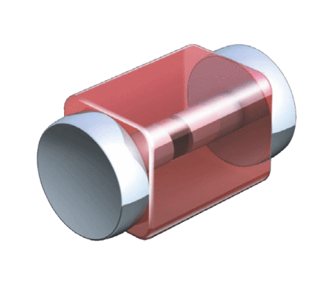
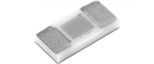
The 5164075 and 5195006 variants belong to the SMD 1206 SC sinterable Pt1000 temperature sensor range, designed for direct integration into power electronic assemblies. Featuring a platinum resistance characteristic of 3850 ppm/K in accordance with DIN EN IEC 60751, these sensors provide reliable temperature measurement close to semiconductor dies and other heat sources, while the substrate arrangement helps maintain electrical isolation.
The AgPd backside is suitable for silver sintering, while the AgPt topside contacts support thick-wire ultrasonic bonding. The sensors are also solderable, offering additional flexibility when selecting an assembly and mounting process. Their compact 1206 format and short potential thermal path make them well suited to space-constrained power electronics applications. Actual response time and thermal performance depend on the final assembly and should be validated in the intended application. Both variants share the same sensing and mechanical specifications and differ primarily in their packaging format.
Range features
A high level overview of what this range offers
- Pt1000 platinum RTD: Provides a standardised resistance-based temperature signal.
- DIN EN IEC 60751 design: Supports integration with established platinum RTD measurement methods.
- Class F 0.6 (2B): Defines the tolerance class across the specified continuous range from -50 °C to +200 °C.
- 3850 ppm/K temperature coefficient: Enables predictable resistance-to-temperature conversion.
- AgPd backside metallisation: Supports silver-sinter attachment to power electronic substrates.
- AgPt topside contacts: Accommodate ultrasonic bonding with Ø300 µm Al H11 thick wire.
- Electrically isolated construction: Allows positioning on or near heat-generating components, subject to system-level insulation design.
- Maximum R₀ drift of 0.23%: Provides quantified stability after the stated endurance tests.
- Self-heating below 0.4 K/mW: Helps limit measurement disturbance when the specified measuring-current range is observed.
- Two packaging options: Wafer-frame and blister-reel formats support different die-attach and automated handling processes.
What’s in this range?
All the variants in the range and a comparison of what they offer
Technical specifications
| Specification | Value |
|---|---|
Product range | SMD 1206 SC Sinter |
Sensor technology | Platinum resistance temperature detector, Pt RTD |
Applicable standard | DIN EN IEC 60751 |
Nominal resistance R₀ | Pt1000, 1,000 Ω at 0 °C |
Tolerance class | F 0.6 (2B) |
Specified continuous temperature range | -50 °C to +200 °C |
Higher-temperature statement | Maximum operating temperature exceeds +200 °C; the exact upper limit and tolerance performance above +200 °C are not defined |
Temperature coefficient | 3850 ppm/K |
Measuring current | 0.1 to 0.3 mA |
Length L1 | 3.1 ±0.15 mm |
Width | 1.5 ±0.15 mm |
Height | 0.55 ±0.15 mm |
Metallised end length L2 | 0.79 mm, reference value |
Self-heating | <0.4 K/mW, unassembled |
Insulation resistance |
|
Maximum R₀ drift | ≤0.23% after the stated standard endurance tests |
High-temperature endurance test | 1,000 hours at +200 °C and ≥0.1 mA |
Damp-heat endurance test | 1,000 hours at +85 °C and 85% relative humidity |
Thermal-cycling test | 1,000 cycles between -40 °C and +150 °C |
Backside attachment | Silver sintering |
Backside metallisation | AgPd thick-film surface |
Recommended sinter paste | ASP 338 or 043 series |
Topside connection | Ultrasonic thick-wire bonding |
Topside metallisation | AgPt thick-film surface |
Recommended bonding wire | Al H11 thick wire, Ø300 µm |
Backside shear result |
|
Topside pull result |
|
Dielectric strength | 7.5 kV, based on theoretical substrate properties and sensor geometry; assembly conditions can reduce the practical value |
Order codes | 5164075 and 5195006 |
Packaging formats | Wafer frame and blister reel |
Blister-reel tape width | 8 mm |
Blister-reel cavity | 3.55 × 1.95 × 0.8 mm |
Blister-reel step and sprocket feature | 4 mm; Ø1.5 mm |
Reel orientation and capacity | Face-up; approximately 4,200 pieces maximum per reel |
Reduced reel quantities | Down to 250 pieces may be available in individual cases |
Storage life | Minimum 9 months in unopened original packaging |
Moisture sensitivity level | MSL-1, unlimited floor-life classification |
Additional options | Other resistance values and tolerances may be available on request |
Material warning | California Proposition 65 warning relating to nickel exposure |
Variant comparison
| Specification | 5164075 | 5195006 |
|---|---|---|
Series | SMD 1206 SC Sinter | SMD 1206 SC Sinter |
Nominal resistance | Pt1000 | Pt1000 |
Tolerance class | F 0.6 (2B) | F 0.6 (2B) |
Temperature range | -50 °C to +200 °C | -50 °C to +200 °C |
Packaging | Wafer frame | Blister reel |
FAQs
for SMD SC (sinterable series)
Use -50 °C to +200 °C as the continuous design range when Class F 0.6 (2B) performance is required. The product information also states that the maximum operating temperature exceeds +200 °C, but it does not define an exact ceiling or an accuracy class beyond +200 °C. Operation above the specified class range should therefore be treated as an application-specific condition rather than a general rated point. Bonding, sinter materials, encapsulation and thermal cycling may become the limiting factors before the platinum element itself. For designs expected to cross +200 °C, confirm the allowable exposure profile and qualify the complete assembly before setting control or protection thresholds.
Attach the backside by silver sintering and make the electrical connections to the topside by ultrasonic thick-wire bonding. The backside uses AgPd thick-film metallisation and was evaluated with ASP 338 or 043 series sinter paste, while the topside uses AgPt metallisation with Ø300 µm Al H11 thick wire. Backside shear results are stated as greater than 10 N/mm² minimum and greater than 20 N/mm² mean; the topside pull result is greater than 210 cN. These values depend on the stated materials and process conditions, so they should not be transferred directly to a different assembly stack. Establish and validate the actual sintering, bonding, cleaning and encapsulation windows on the intended substrate.
Use a measuring current between 0.1 and 0.3 mA, then verify self-heating in the finished thermal stack. At 0 °C, a Pt1000 element dissipates about 0.01 mW at 0.1 mA and 0.09 mW at 0.3 mA. With the unassembled self-heating coefficient below 0.4 K/mW, those figures correspond to less than approximately 0.004 K and 0.036 K respectively under the stated test condition. Resistance and power rise with temperature when a constant current is used, while the mounted thermal path may behave differently from the unassembled element. Choose the lower end of the current range where the measurement uncertainty budget is tight, and confirm the final error experimentally.
The stated long-term stability limit is a maximum R₀ drift of 0.23% after the defined standard tests. For a Pt1000 sensor, 0.23% corresponds to 2.3 Ω; using 3.85 Ω/K near 0 °C, that is approximately 0.6 K if treated solely as an equivalent resistance shift rather than total measurement error. The tests comprise 1,000 hours at +200 °C with at least 0.1 mA, 1,000 hours at +85 °C and 85% relative humidity, and 1,000 cycles between -40 °C and +150 °C. These results support component qualification but do not predict every mounting or mission profile. Include interface drift, electronics error and any calibration interval in the system-level error budget.
The element provides an insulation resistance above 1,000 MΩ at 20 °C and a stated dielectric strength of 7.5 kV. The dielectric figure is based on theoretical substrate properties and the given sensor geometry, so it is not a guaranteed withstand rating for the completed assembly. Potting material, the potting meniscus, contamination, bond-wire geometry and processing can reduce the practical value. Creepage, clearance and isolation coordination must therefore be designed at system level rather than inferred from the sensor alone. Where the part is placed near a high-side power semiconductor, perform high-potential, humidity and thermal-cycling tests on the final stack.
Choose 5164075 for wafer-frame supply and 5195006 for blister-reel supply; the sensing, dimensional and temperature data are otherwise common. The blister format uses 8 mm tape with a 3.55 × 1.95 × 0.8 mm cavity, 4 mm step and Ø1.5 mm sprocket feature. It is supplied face-up with a stated maximum of approximately 4,200 pieces per reel, while lower quantities down to 250 pieces may be possible in individual cases. Wafer-frame supply is generally aligned with die-attach handling, whereas reel supply can suit automated component placement, subject to equipment compatibility. Both formats require process review for pick-up tooling, orientation and placement force.
Yes, the construction is intended for mounting on power electronic boards close to a heat source or semiconductor die. Its 3.1 × 1.5 × 0.55 mm body allows local placement, while backside silver sintering creates a short conductive thermal interface and the topside contacts keep the electrical connection above the substrate. No numerical response-time value is defined, so the actual dynamic behaviour must be established with the selected substrate, sinter thickness, encapsulation and cooling conditions. Thermal modelling should be followed by a step-response test using the intended readout current and filtering. This confirms whether the sensor follows the local die region closely enough for control, derating or protection.