InSb Infrared Detectors
- Technology
- Infrared photodetectors
- Partner
- Infrared Associates
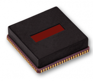
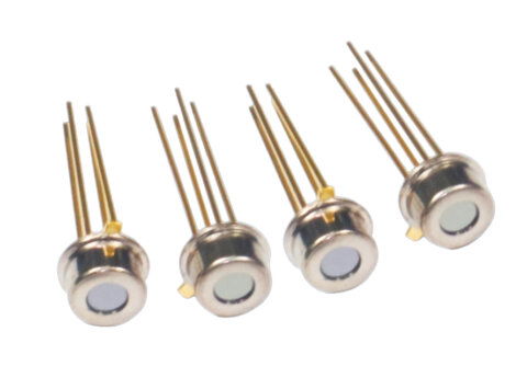
InSb infrared detectors are photovoltaic mid-infrared photodiodes built on Indium Antimonide, engineered to detect wavelengths roughly from 1 µm up to 5.5 µm. They operate at cryogenic temperatures (typically around 77 K using liquid nitrogen cooling) to drastically reduce thermal noise, allowing the devices to achieve background-limited sensitivity. Each detector is a p–n junction that generates an electrical signal (photocurrent) when IR radiation is absorbed, often requiring no external bias under optimal conditions. In practice, a low-noise preamplifier is used to read out the small signal and can apply a slight reverse bias if needed to maintain zero-offset under high infrared background. Standard InSb detectors come in two active area sizes (approximately 1×1 mm and 2×2 mm), letting engineers choose between a smaller or larger photodiode depending on the desired field of view and sensitivity. These detectors are housed in vacuum-sealed cryogenic dewars (with sapphire IR windows) to maintain the cold operating temperature for up to 8–12 hours. Typical application areas include medical thermography, thermal imaging systems, infrared spectroscopy, radiometry instruments, scientific research and IR microscopy – essentially any use case that demands detection of very weak mid-wave IR signals with high precision and low noise.
Working principle of the InSb Infrared Detectors
The photovoltaic effect is the generation of potential over the p-n transition when radiation of the correct wavelength hits it. When the photon flow irradiates the transition, electron-hole pairs are formed when the photon energy exceeds the bandgap.
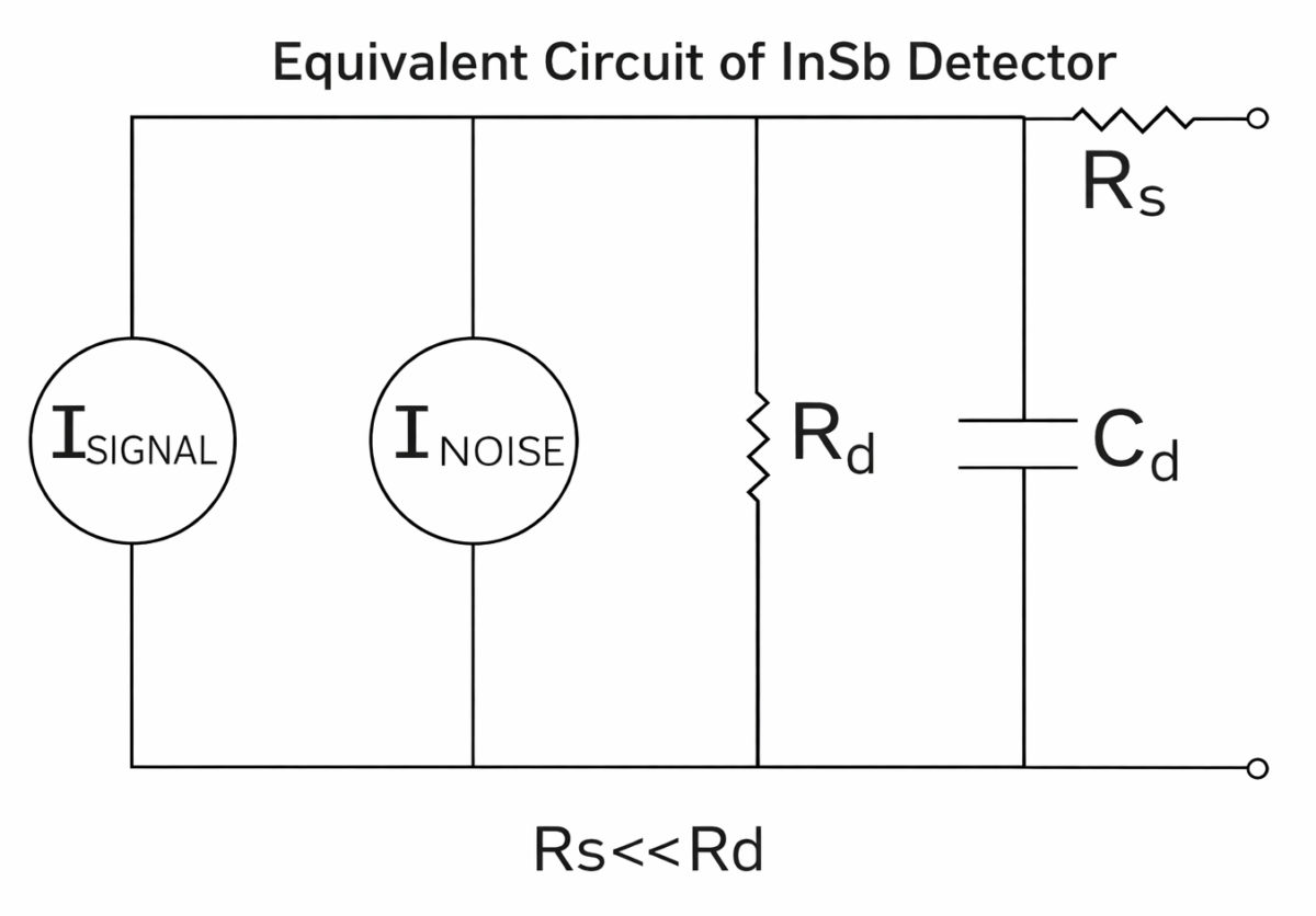
The field brings electrons from the p-range to the n-range and the holes from the n-range to the p-range. This process makes the p-region positive and the n region negative and generates a current flow in an external circuit. An image of the InSb detector is displayed on the right. This consists of both a signal and noise current generator in parallel with a resistive and capacitive term.
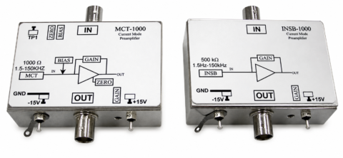
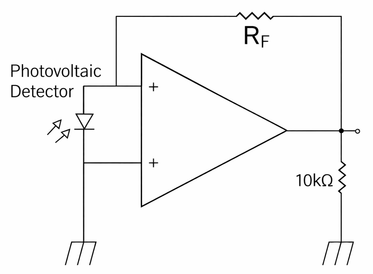
With the detector, a suitable preamplifier can be offered, which is optimally adapted to the selected detector.
Range features
A high level overview of what this range offers
- Mid-infrared spectral sensitivity (∼1–5.5 µm) – Enables detection of mid-wave IR emissions for thermal imaging, gas analysis, and other MWIR applications
- Photovoltaic InSb photodiode design – P–n junction structure ensures low inherent noise and stable performance without requiring constant bias
- Background-limited performance (BLIP) – Detector noise floor is limited by ambient infrared background, resulting in maximal sensitivity under normal operating conditions
- High detectivity and responsivity – Achieves D* > 1×10¹¹ and > 3 A/W (peak), meaning it can discern extremely weak IR signals and slight temperature differences
- Cryogenic 77 K operation – Cooling the detector to liquid-nitrogen temperature drastically reduces thermal noise, unlocking orders-of-magnitude improvement in signal-to-noise ratio
- Flexible LN2 dewars and window – Offered with side-looking or down-looking cryogenic dewars (8 hr or 12 hr hold time) and a sapphire window for compatibility with various optical setups
- Multiple active area options – Available in 1 mm² or 4 mm² photodiode sizes (and custom arrays on request) to suit different sensitivity, aperture, or field-of-view requirements
- Custom configurable – Detectors can be tailored or supplied in special configurations (e.g. integrated with cooled filters or alternative packaging) to meet specific project needs
Downloads
for InSb Infrared Detectors
What’s in this range?
All the variants in the range and a comparison of what they offer
| Specification | IS-1.0 Detector | IS-2.0 Detector |
|---|---|---|
Active area (mm) | 1 × 1 (single element) | 2 × 2 (single element) |
Spectral response range | ~1 µm to 5.5 µm | ~1 µm to 5.5 µm |
Peak detectivity, D* (cm·Hz1/2/W) | ≥ 1.0 × 10¹¹ (300 K bkg, 60° FOV) | ≥ 1.0 × 10¹¹ (100 K bkg, 60° FOV) |
Peak responsivity (A/W @ peak λ) | ≥ 3 | ≥ 3 |
Capacitance (pF @ 77 K) | ~350 | ~1500 |
Short-circuit current (µA @ 300 K background) | ~8 | ~30 |
Operating temperature (K) | 77 | 77 |
Window material | Sapphire (standard) | Sapphire (standard) |
FAQs
for InSb Infrared Detectors
InSb infrared detectors are sensitive to wavelengths roughly from about 1 µm up to 5.5 µm. This range covers most of the mid-wave infrared (MWIR) band. The detector’s long-wavelength cutoff is around 5.3–5.5 µm, determined by the bandgap of Indium Antimonide at cryogenic temperatures. Shorter wavelengths down to ~1 µm are also detected (photons with energy above the bandgap will generate a signal), meaning these photodiodes span portions of the near-IR into the entire MWIR region.
InSb detectors must be cryogenically cooled (typically to about 77 K, the boiling point of liquid nitrogen) to achieve their high sensitivity. At room temperature (300 K), an InSb photodiode would suffer from extremely high dark current and thermal noise due to the material’s narrow bandgap. Cooling the detector to 77 K (or similar low temperatures) freezes out much of this thermal noise and reduces dark current dramatically. The result is that the detector can operate in a background-limited regime, where the dominant noise source is the external infrared background rather than the detector’s own thermal noise. In practice, these detectors are often integrated into liquid nitrogen dewars or closed-cycle refrigeration systems to maintain the necessary low temperature during use.
Background-limited infrared performance (BLIP) means that the detector’s noise is predominantly caused by background radiation (ambient infrared from the environment or scene), rather than by the detector’s internal noise sources. In other words, once the InSb detector is properly cooled, its own readout noise and dark current noise become so low that the remaining noise floor is set by the statistical fluctuations of incoming background photons. This is actually a desirable situation because it implies the detector is operating at its theoretical sensitivity limit given the environment. A BLIP detector can achieve very high detectivity since any further reduction in internal noise wouldn’t significantly improve performance – only reducing the background (for example, narrowing the field of view or using spectral filters) would yield a noticeable sensitivity improvement. Engineers sometimes take advantage of this by using cooled apertures or interference filters to limit the background reaching the detector, thus further enhancing the signal-to-noise ratio in specific measurement conditions.
These Indium Antimonide detectors offer very high sensitivity in the mid-IR. Their peak detectivity D is on the order of 10^11 cm·Hz1/2/W (or higher) at the optimal wavelength (around the 5 µm region) when operated at 77 K with a typical 300 K background and ~f/1 collection optics (60° field of view). In practical terms, D > 1×10^11 indicates the detector can discern extremely low radiant flux levels – it’s one of the highest D values for mid-wave IR photodiodes. The peak responsivity is generally above 3 A/W, meaning the detector produces more than 3 amperes of photocurrent per watt of incident mid-IR radiation at its peak response wavelength. This high responsivity translates to strong electrical output even for modest incoming IR signals, which is beneficial for applications like spectroscopy or thermography where signal levels can be very small. It’s worth noting that both D and responsivity tend to be maximum at the detector’s long-wavelength end (just before the 5.5 µm cutoff), and they will slightly decrease at shorter wavelengths. Overall, these figures highlight that InSb detectors are extremely sensitive devices suitable for detecting minute IR signals.
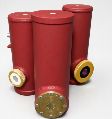
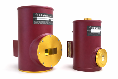
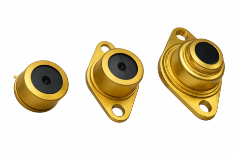
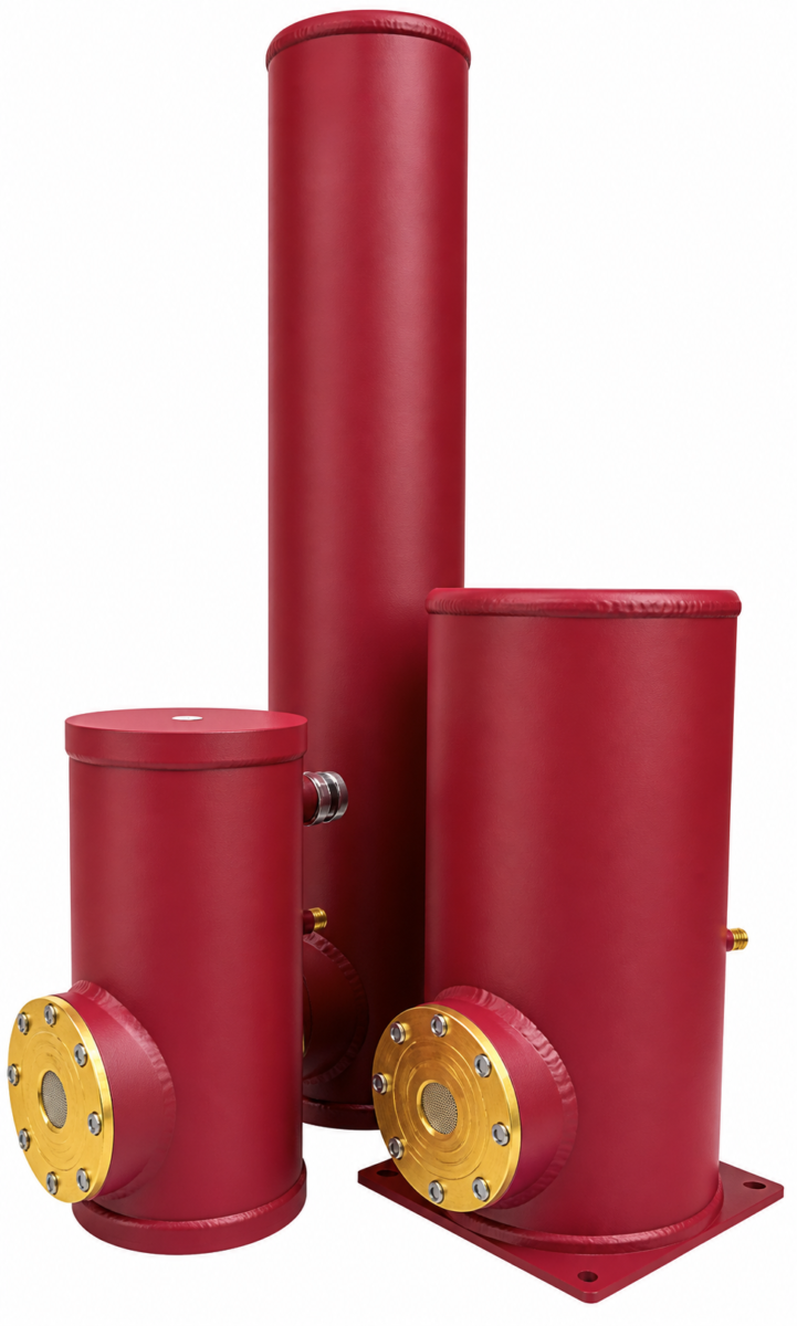
The standard packaging for these InSb detectors is a hermetic cryogenic dewar with a built-in infrared-transparent window. Typically, a sapphire window is used as it is robust and passes the 1–5.5 µm spectrum. There are a few dewar configurations offered: a side-looking metal dewar (denoted MSL) and a down-looking metal dewar (MDL), each available with either approximately 8-hour or 12-hour hold time (the hold time indicates how long the liquid nitrogen coolant will last before needing a refill). For example, an “MSL-8” dewar means side-looking geometry with an ~8 hour LN2 hold. These options allow users to choose a geometry that best fits their optical setup – side-looking dewars are often used when the detector needs to view horizontally out of the package, whereas down-looking dewars view through the bottom (useful for upward-facing optical paths or mounting onto optical benches). All standard dewars are liquid-nitrogen cooled to reach the ~77 K operating temperature. Additionally, the detectors can be integrated with cooled optical elements if needed – for instance, some configurations allow installing a cooled interference filter or aperture stop inside the dewar in front of the detector. This can limit the spectral or spatial field of view, further reducing background noise for specific measurement requirements. For applications where using liquid nitrogen is impractical, these detectors can alternatively be used with closed-cycle cryocooler systems (or Stirling coolers) designed to reach similar temperatures, and the manufacturer can provide guidance or packaging solutions for those scenarios as well.
Under normal operating conditions, InSb photodiode detectors do not require any external bias voltage – they are used in photovoltaic mode (zero bias). When cooled and at equilibrium, the photodiode’s optimal operating point is at zero volts bias, and the detector produces a current in response to incoming infrared radiation. However, practically, you will almost always use a transimpedance preamplifier or similar low-noise amplifier with the detector to convert that photocurrent into a measurable voltage signal and to provide impedance matching. The preamplifier not only boosts the minute signal but can also apply a slight reverse bias if needed for certain conditions. In scenarios with very high background infrared levels (for example, if the detector is exposed to a wide field or warm scene), the photodiode may produce a constant offset current that pushes it away from the optimal zero-bias point. In such cases, applying a small reverse bias (through the amplifier circuit) re-centres the operating point and maximizes dynamic range. The manufacturer offers a dedicated preamplifier designed for these InSb detectors, which provides adjustable bias (0 to +2.5 V typically) and variable gain. Using the recommended preamp or an equivalent low-noise amplifier is important – it ensures the detector plus amplifier system remains detector-noise-limited, meaning the amplifier’s noise is lower than the detector’s own noise. In summary, you don’t need to bias the detector for it to work, but you do need a good amplifier to read out its tiny current, and that amplifier can introduce a bias if the application calls for it.
InSb infrared detectors are used in a wide array of scientific, industrial, and military applications whenever high-sensitivity mid-wave IR detection is required. Some prominent examples include:
- Medical thermography: InSb detectors can capture minute temperature differences in medical diagnostics or skin surface temperature mapping, thanks to sensitivity in the 3–5 µm band where human body radiation is significant.
- Thermal imaging and surveillance: Many MWIR thermal cameras and night-vision systems (especially older generation or high-end cooled systems) use InSb focal plane arrays or single detectors scanning a scene. A single-element InSb detector might be used in a scanning thermal imager or as a reference sensor in calibrated thermal imaging equipment.
- Spectroscopy: InSb photodiodes serve as detectors in IR spectrometers for chemistry, gas analysis, and materials science. They are suitable for detecting absorption or emission lines in the 2–5 µm range (for example, for hydrocarbon gases or other molecular signatures) with very low detection limits.
- Radiometry and IR standards: Because of their stable and predictable response, cooled InSb detectors are often used in radiometric measurements and calibration systems as a reference detector for mid-infrared power or energy.
- Scientific research and IR microscopy: In laboratories, InSb detectors might be found in IR microscope attachments, laser measurement setups (for lasers operating in the 1–5 µm range), or any experiment where detecting faint mid-IR signals is necessary. Their fast response also allows them to be used in time-resolved measurements of IR phenomena.
In all these applications, the key reasons for choosing an InSb detector are its high sensitivity, low noise (when cooled), and strong performance exactly in the mid-wave infrared region of interest.
InSb photodiode detectors have a fast response, but the overall bandwidth is influenced by their junction capacitance and the readout electronics. A small-area InSb detector (like the 1×1 mm element) combined with a standard preamplifier typically provides a bandwidth on the order of hundreds of kilohertz. For example, a conventional transimpedance amplifier configuration might support a frequency response from DC up to about 150 kHz (this is often limited by the RC time constant of the detector’s capacitance and the feedback resistor in the amp). However, with special high-speed configurations, the bandwidth can be extended into the low megahertz range. By using a smaller detector (to reduce capacitance), applying a slight reverse bias (which also reduces the effective capacitance and speeds up carrier collection), and using a high-speed amplifier design, bandwidths up to around 1–5 MHz are achievable. In fact, the manufacturer notes that with custom configurations, bandwidths as high as 5 MHz are available for InSb detectors. It’s important to match the preamplifier and bias settings to the desired speed: achieving the top-end MHz bandwidth might come at the expense of some sensitivity (since introducing bias can increase noise slightly). For most applications like spectroscopy or thermal imaging, the standard <0.2 MHz bandwidth is more than sufficient. But for time-resolved infrared laser measurements or rapid scanning systems, the detectors can be configured for those higher frequencies.