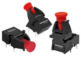
FR50MVIR 650 nm DC-50 MBd 50 m RedLink® POF Vertical Receiver
- Technology
- Plastic Optical Fibre (POF) components
- Partner
- Firecomms
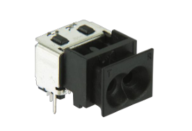
The FR50MVIR combines a photodiode and receiver IC in a miniature optical connector package with a vertical fibre interface. Its inverting electrical output supports PCB designs that require active-low logic. The receiver accepts plug-terminated plastic optical fibre or 200 µm plastic-clad silica fibre. Optical performance is characterised with transmitters operating from 635 to 680 nm, covering commonly used 650 nm links. Supported data rates extend from static DC states to 50 MBd, with specified pulse-width distortion and propagation-delay limits. The device operates from either a 3.3 V or 5 V supply rail with ±10% tolerance across temperatures from −40 °C to +85 °C. Applications include industrial automation, serial communications, voltage isolation and optical links carrying RS232, RS485, CAN bus, Modbus or PROFIBUS signals.
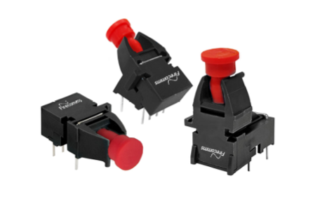
The FR50MVIR is the vertical, inverting member of the RedLink® FR50MxxR receiver range. It provides optical-to-electrical conversion for POF and 200 µm PCS links while supporting static states and digital signalling up to 50 MBd. Its integrated construction, dual-voltage operation and industrial temperature rating make it suitable for compact control, communication and isolation interfaces.
Range features
A high level overview of what this range offers
- Integrated photodiode and receiver IC – Can reduce the external circuitry required for optical-to-electrical conversion.
- DC to 50 MBd operation – Supports static states and digital signals with unit intervals down to 20 ns.
- Vertical inverting configuration – Provides vertical fibre entry with an output logic state inverted relative to the optical input.
- POF and 200 µm PCS compatibility – Supports different fibre types for short and extended industrial links.
- 50 m POF link distance – Accommodates machine, cabinet and production-line communication runs, depending on installation conditions.
- 3.3 V and 5 V supply operation – Eases integration with different industrial logic and controller platforms.
- Push-pull TTL-compatible CMOS output – Provides a direct digital output within the stated loading conditions.
- Specified pulse-width distortion – Supports pulse integrity in continuous and burst-mode NRZ data links.
- −40 °C to +85 °C operation – Allows use across the stated industrial temperature range.
- RoHS compliance and UL 94 V-0 material rating – Supports environmental and flame-retardancy requirements in equipment design.
Downloads
for FR50MVIR 650 nm DC-50 MBd 50 m RedLink® POF Vertical Receiver
What’s in this range?
All the variants in the range and a comparison of what they offer
Receiver electrical and optical characteristics
| Parameter | Symbol | Minimum | Typical | Maximum | Unit | Conditions |
|---|---|---|---|---|---|---|
Supply current | I_CC | — | 20 | 25 | mA | Recommended transmitter and receiver circuits |
Wake-up delay | t_power-on | — | 40 | — | µs | Measured after V_CC exceeds 2.75 V |
High-level output voltage | V_OH | V_CC − 0.05 | — | V_CC | V | I_OH max. = 40 µA |
Low-level output voltage | V_OL | 0 | — | 0.05 | V | I_OL max. = 1.6 mA |
Optical power high | P_H | −22 | — | +2 | dBm | Peak optical input power |
Optical power low | P_L | — | — | −40 | dBm | Peak optical input power |
Data rate | — | DC | — | 50 | MBd | Minimum UI = 20 ns; maximum signal frequency = 25 MHz |
Output rise time, 10% to 90% | t_r | — | — | 5 | ns | Recommended receiver circuit |
Output fall time, 90% to 10% | t_f | — | — | 5 | ns | Recommended receiver circuit |
Pulse-width distortion, P_H from −20 to +2 dBm | PWD | −4 | — | +4 | ns | 50 MBd NRZ PRBS7 data |
Pulse-width distortion, P_H from −22 to −20 dBm | PWD | −6 | — | +6 | ns | 50 MBd NRZ PRBS7 data |
Initial pulse-width distortion, first to third pulse | PWD_init | −7 | — | +14 | ns | Minimum optical pulse width of 20 ns |
High-to-low propagation delay | t_PropDly-HL | — | — | 50 | ns | Recommended receiver circuit |
Low-to-high propagation delay | t_PropDly-LH | — | — | 50 | ns | Recommended receiver circuit |
Optical sensitivity range | λ_R | 400 | — | 900 | nm | Performance values characterised from 635 to 680 nm |
The characteristics are validated from −40 °C to +85 °C with 3.3 V or 5 V supply rails at ±10%. Optical input values are peak rather than average power; for 50% duty-cycle data, peak optical power is twice the average power. Electrical timing is evaluated with a 50 kΩ load resistance and total load capacitance of 15 pF. Pulse-width distortion is measured using 50 MBd NRZ PRBS7 data at a bit error rate no greater than 10⁻⁹.
Pin assignment
| Pin | Function | Symbol |
|---|---|---|
1 | Receiver output | V_O |
2 | Receiver ground | GND |
3 | Receiver supply | V_CC |
4 | No connect | NC |
5 | Retaining pin | GND |
8 | Retaining pin | GND |
Pin 4 is electrically isolated internally. It may be connected to pin 1 for compatibility with an existing PCB layout; otherwise, grounding pin 4 is recommended. Pins 5 and 8 provide mechanical mounting and retention and should be connected to ground.
FR50MxxR variant matrix
| Specification | FR50MHNR | FR50MHIR | FR50MVNR | FR50MVIR | FR50MWNR | FR50MWIR |
|---|---|---|---|---|---|---|
Package orientation | Horizontal | Horizontal | Vertical | Vertical | 30° tilted | 30° tilted |
Output logic | Non-inverting | Inverting | Non-inverting | Inverting | Non-inverting | Inverting |
Rated data rate | 50 MBd | 50 MBd | 50 MBd | 50 MBd | 50 MBd | 50 MBd |
Absolute maximum ratings
| Parameter | Symbol | Minimum | Maximum | Unit |
|---|---|---|---|---|
Storage temperature | T_stg | −40 | +85 | °C |
Operating temperature | T_op | −40 | +85 | °C |
Soldering temperature | T_sld | — | +260 | °C |
Receiver supply voltage | V_CC | −0.5 | +7 | V |
Receiver output current | I_O | −16 | +16 | mA |
The +260 °C soldering limit applies for 10 seconds on one occasion and at least 2.2 mm from the lead root. Absolute maximum values are stress ratings and are not normal operating conditions.
Regulatory and storage compliance
| Parameter | Symbol | Standard | Level or status |
|---|---|---|---|
Human Body Model contact ESD | HBM | MIL-STD-883 | Level 2, 4 kV |
Radiated emissions immunity | V m⁻¹ | IEC 61000-4-3 | 15 V m⁻¹ |
UL certification | UL | UL 60950-1 | File E362227 |
Moisture sensitivity | MSL | J-STD-020 | Level 2a; four-week floor life |
Restriction of hazardous substances | RoHS | Directive 2011/65/EU, including Amendment 2015/863 | Certified compliant |
FAQs
for FR50MVIR 650 nm DC-50 MBd 50 m RedLink® POF Vertical Receiver
Set the link budget so that the peak optical-high power reaching the receiver remains between −22 and +2 dBm, while the optical-low state is no higher than −40 dBm. The receiver is characterised with transmitters emitting between 635 and 680 nm, so a 650 nm source lies within the characterised band; the broader 400 to 900 nm sensitivity range does not imply identical performance at every wavelength. The optical limits refer to peak rather than average power, and peak power is twice the average for 50% duty-cycle data. The calculation should include fibre attenuation, connectors, temperature, transmitter tolerance, contamination and ageing. For a proposed 50 m POF or 300 m PCS link, verify both the minimum received high level and maximum permitted input power under worst-case conditions.
The receiver can operate from either a 3.3 V or 5 V DC supply, with a permitted rail variation of ±10%. Its supply current is typically 20 mA and may reach 25 mA, so the regulator and power-distribution network should be sized for the maximum value. A 100 nF capacitor should be fitted close to the V_CC pin of every receiver. The recommended supply filter uses two 10 µF capacitors and a 1 µH inductor to reduce noise coupled from other components on the same rail. Where several receivers are positioned close together, the larger filter network may be shared, but each device still requires its own local 100 nF decoupling capacitor.
The FR50MVIR produces an electrical logic state that is inverted relative to the detected optical input. When light is present, the normal operating output is therefore low; when light is absent and the input is below the optical-low threshold, the output is high. During startup, the output remains in a high-impedance state as the supply approaches approximately 2.8 V. The listed wake-up delay is 40 µs, after which the output changes to the correct logic state for the optical input. If the supply falls below approximately 2.6 V, the output immediately returns to high impedance, which should be considered when designing reset, pull-state and fault-detection logic.
At 50 MBd, the minimum unit interval is 20 ns and the maximum alternating-pattern frequency is 25 MHz. Output rise and fall times are each specified at no more than 5 ns, while high-to-low and low-to-high propagation delays are each limited to 50 ns. Pulse-width distortion is limited to ±4 ns when the optical-high level is between −20 and +2 dBm, increasing to ±6 ns near the lower sensitivity region from −22 to −20 dBm. The first three pulses can exhibit a wider range from −7 to +14 ns, with the first pulse representing the least favourable case. Protocol timing, sampling points and receiver-to-controller skew should therefore be checked against both steady-state and initial-pulse limits.
The optical interface accepts plastic optical fibre and 200 µm plastic-clad silica fibre. Step-index POF links can extend to 50 metres, while links using 200 µm PCS fibre can reach 300 metres, although both figures depend on installation conditions. The receiver can be used in optical physical layers carrying RS232, RS485, CAN bus, Modbus or PROFIBUS communications where the signal rate remains within the DC to 50 MBd range. It performs optical-to-electrical conversion and does not itself implement protocol framing, bus arbitration or line coding. The chosen transmitter, fibre, connector losses and interface circuitry must therefore be validated as a complete link rather than treating the receiver as a protocol converter.
The receiver is not suitable for infrared or vapour-phase reflow soldering. Its one-time soldering limit is +260 °C for 10 seconds, measured at least 2.2 mm from the lead root, and non-halogenated water-soluble flux is recommended. The dust plug should remain fitted throughout soldering, washing and drying to protect the active optical area. Alcohol-based cleaning agents such as methyl, isopropyl or isobutyl alcohol may be used, while acetone, ethyl acetate and phenol-based products are not permitted. The device is classified as MSL 2a and may remain under normal factory conditions below 30 °C and 60% relative humidity for up to 672 hours after opening. An unopened moisture-barrier bag has a stated shelf life of 24 months below 40 °C and 90% relative humidity.
The receiver is rated to operate and be stored from −40 °C to +85 °C, allowing the same temperature limits to be applied during equipment qualification. Contact electrostatic discharge is rated to Human Body Model Level 2 at 4 kV under MIL-STD-883. Radiated immunity is specified at 15 V m⁻¹ under IEC 61000-4-3, which provides a defined reference point for electromagnetic compatibility planning. The device carries UL 60950-1 certification under file E362227 and is compliant with the stated RoHS directive and amendment. Its housing material is rated UL 94 V-0, while storage and assembly controls are defined by the MSL 2a classification. These component-level ratings should be considered alongside the enclosure, PCB, cabling and system-level compliance requirements.