CT-0155TBR-Kx7C-A 1550 nm DFB/1310 nm PIN 60 km 155 Mb/s 1×9 Bi-Di Transceiver
- Technology
- Optical transceivers
- Partner
- Coretek
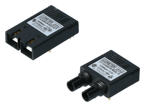
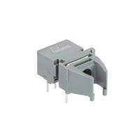
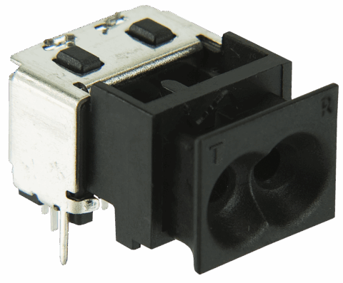
The CT-0155TBR-Kx7C-A is a board-mounted, single-fibre optical module for 155 Mb/s NRZ communication over single-mode fibre. It combines a 1550 nm DFB transmitter with a 1310 nm PIN receiver and routes both directions through one SC receptacle. The fixed 1×9 footprint and differential PECL interface are intended for equipment designed around this established transceiver format. Two electrical variants are available for integration with either 3.3 V or 5 V system rails. With an optical output range of −5 to 0 dBm and receiver sensitivity of up to −34 dBm, the module is specified for links up to 60 km when the complete optical budget remains within its limits. Its −40 to +85 °C operating range supports installations exposed to wide ambient temperature changes, provided the final thermal and power design is verified. Typical applications include Fast Ethernet, FDDI, ATM/SONET OC-3, SDH STM-1 and optical-electrical interface conversion.
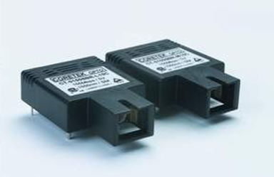
Range features
A high level overview of what this range offers
- 1550 nm DFB transmitter and 1310 nm PIN receiver: Enables bidirectional communication over one single-mode fibre when paired with a complementary-wavelength module.
- 155 Mb/s NRZ operation: Supports Fast Ethernet, FDDI and ATM/SONET OC-3 or SDH STM-1 applications.
- Up to 60 km specified reach: Accommodates long-distance single-mode fibre links within the available optical budget.
- Single SC receptacle: Combines transmit and receive paths in one fibre connection.
- Industry-standard 1×9 footprint: Supports integration into established board layouts using this fixed transceiver format.
- 3.3 V and 5 V variants: Allows selection to match the host equipment power rail.
- Differential PECL interface: Provides separate transmit, receive and signal-detect connections for board-level integration.
- −40 to +85 °C operation: Supports equipment installed across an extended ambient temperature range.
- RoHS-compliant, lead-free construction: Assists with restricted-substance requirements.
- Laser Class 1 design aligned with EN 60825-1: Supports eye-safety planning, subject to final equipment assessment.
Downloads
for CT-0155TBR-Kx7C-A 1550 nm DFB/1310 nm PIN 60 km 155 Mb/s 1x9 Bi-Di Transceiver
What’s in this range?
All the variants in the range and a comparison of what they offer
Technical specifications
| Category | Parameter | Symbol | Minimum | Typical / nominal | Maximum | Unit | Conditions / notes |
|---|---|---|---|---|---|---|---|
Absolute maximum | Storage temperature | TS | −40 | — | 85 | °C | — |
Absolute maximum | Supply voltage | VCC | 0 | — | 6 | V | — |
Absolute maximum | Lead soldering temperature | TSOLD | — | — | 260 | °C | Maximum 10 seconds on the lead |
Absolute maximum | Data input voltage | — | 0 | — | VCC | V | — |
Operating condition | Ambient operating temperature | TA | −40 | — | 85 | °C | — |
Operating condition | 5 V supply range | VCC | 4.75 | — | 5.25 | V | CT-0155TBR-K17C-A |
Operating condition | 3.3 V supply range | VCC | 3.10 | — | 3.50 | V | CT-0155TBR-K27C-A |
Electrical – transmitter | Transmitter supply current | ICCT | — | — | 200 | mA | — |
Electrical – transmitter | Data input current, low | IIL | −350 | — | — | µA | — |
Electrical – transmitter | Data input current, high | IIH | — | — | 350 | µA | — |
Electrical – transmitter | Data input voltage, low | VIL − VCC | −1.810 | — | −1.620 | V | Compatible with 10K, 10KH and 100K ECL/PECL outputs |
Electrical – transmitter | Data input voltage, high | VIH − VCC | −1.025 | — | −0.880 | V | Compatible with 10K, 10KH and 100K ECL/PECL outputs |
Electrical – receiver | Receiver supply current | ICCR | — | — | 100 | mA | — |
Electrical – receiver | Data output voltage, low | VOL − VCC | −1.810 | — | −1.620 | V | Compatible with 10K, 10KH and 100K ECL/PECL inputs |
Electrical – receiver | Data output voltage, high | VOH − VCC | −1.025 | — | −0.880 | V | Compatible with 10K, 10KH and 100K ECL/PECL inputs |
Electrical – signal detect | Output voltage, low | VOL − VCC | −1.810 | — | −1.620 | V | PECL output |
Electrical – signal detect | Output voltage, high | VOH − VCC | −1.025 | — | −0.880 | V | High level indicates a received optical signal |
Transmitter optical | Optical output power | PO | −5 | — | 0 | dBm | Average power coupled into 9/125 µm single-mode fibre |
Transmitter optical | Extinction ratio | ER | 10 | — | — | dB | — |
Transmitter optical | Centre wavelength | λc | 1530 | 1550 | 1570 | nm | — |
Transmitter optical | Spectral width at −20 dB | Δλ | — | — | 1 | nm | — |
Transmitter optical | Side-mode suppression ratio | SMSR | 30 | — | — | dB | — |
Transmitter optical | Optical rise time, 10–90% | tr | — | — | 2.0 | ns p-p | Tested with a 12.5 MHz square-wave pattern |
Transmitter optical | Optical fall time, 10–90% | tf | — | — | 2.0 | ns p-p | Tested with a 12.5 MHz square-wave pattern |
Transmitter optical | Output eye | — | — | Compliant with ITU-T G.957 | — | — | — |
Receiver optical | Maximum input optical power | Pmax | −3 | — | — | dBm | Measured using a 2²³−1 PRBS at BER below 10⁻¹⁰ |
Receiver optical | Receiver sensitivity | Pmin | — | — | −34 | dBm | Measured using a 2²³−1 PRBS at BER below 10⁻¹⁰ |
Receiver optical | Operating wavelength | λ | 1270 | 1310 | 1350 | nm | — |
Receiver optical | Signal detect, asserted | PA | — | — | −34 | dBm | Low-to-high transition |
Receiver optical | Signal detect, deasserted | PD | −47 | — | — | dBm | High-to-low transition |
Receiver optical | Signal-detect hysteresis | PA − PD | 0.5 | — | 4 | dB | — |
Variant comparison
| Specification | Variant 1 | Variant 2 |
|---|---|---|
Model number | CT-0155TBR-K17C-A | CT-0155TBR-K27C-A |
Operating voltage and SD output | 5 V PECL DC/DC | 3.3 V PECL DC/DC |
Link distance | 60 km | 60 km |
Transmit/receive wavelength | 1550 nm DFB / 1310 nm | 1550 nm DFB / 1310 nm |
Optical output power | −5 to 0 dBm | −5 to 0 dBm |
Receiver sensitivity | ≤ −34 dBm | ≤ −34 dBm |
Pin allocation
| Pin or item | Symbol | Function |
|---|---|---|
Mounting posts | — | Mechanical attachment to the circuit board; may connect to chassis ground but should not connect to circuit ground |
1 | VEER | Receiver signal ground |
2 | RD+ | Receiver data non-inverted differential output |
3 | RD− | Receiver data inverted differential output |
4 | SD | PECL signal-detect output; a high level indicates a received optical signal |
5 | VCCR | Receiver power supply |
6 | VCCT | Transmitter power supply |
7 | TD− | Transmitter data inverted differential input |
8 | TD+ | Transmitter data non-inverted differential input |
9 | VEET | Transmitter signal ground |
FAQs
for CT-0155TBR-Kx7C-A 1550 nm DFB/1310 nm PIN 60 km 155 Mb/s 1×9 Bi-Di Transceiver
Choose the CT-0155TBR-K17C-A for a 5 V host rail and the CT-0155TBR-K27C-A for a 3.3 V rail. The 5 V version operates from 4.75 to 5.25 V, while the 3.3 V version accepts 3.10 to 3.50 V; both provide PECL differential data and PECL signal detect. Maximum supply currents are 200 mA for the transmitter and 100 mA for the receiver, giving a combined module allowance of up to 300 mA before design margin is added. The transmitter and receiver have separate supply pins, so each path should receive suitable local decoupling. Variant selection should follow the host logic, available power and thermal design rather than optical reach, which is identical for both versions.
Use the worst-case optical limits rather than treating 60 km as an unconditional operating distance. A minimum transmitter output of −5 dBm combined with receiver sensitivity of −34 dBm produces a 29 dB power budget before accounting for fibre attenuation, connectors, splices, ageing, temperature effects and maintenance margin. At the other end of the range, a 0 dBm transmitter and −3 dBm maximum receiver input indicate that a very short or unusually low-loss path may require at least 3 dB of attenuation to avoid receiver overload. Both directions of the link must be calculated independently. The opposite endpoint must also use complementary wavelengths, transmitting at 1310 nm and receiving at 1550 nm.
It can be used where the host equipment provides compatible NRZ signalling and PECL electrical levels within the module’s 155 Mb/s operating range. Supported applications include 100BASE-FX, FDDI PMD, ATM, SONET OC-3 and SDH STM-1, while the transmitter output eye is specified against ITU-T G.957. The module performs optical-to-electrical and electrical-to-optical conversion but does not replace the host protocol, framing or system-control circuitry. Clocking, coding, link-state handling and fault management must therefore be implemented elsewhere in the equipment. Designers should verify the exact host line rate, jitter requirements and termination arrangement before approving the interface.
The host must provide compatible PECL or ECL levels and use termination appropriate to the selected supply voltage and system chipset. Transmitter input levels are specified relative to VCC, with low levels from −1.810 to −1.620 V and high levels from −1.025 to −0.880 V; the receiver and signal-detect outputs use the same voltage ranges. The interface is compatible with 10K, 10KH and 100K ECL or PECL logic families. Differential data traces should be routed as matched, controlled-impedance pairs with minimal discontinuities and suitable return paths. Final bias and termination component values must be selected for the host receiver or transmitter rather than assumed to be universal.
Yes, the specified ambient operating range is −40 to +85 °C, and the storage-temperature limits cover the same range. This makes the transceiver suitable for equipment exposed to wide temperature changes, provided its case temperature, airflow and electrical loading remain controlled within the completed assembly. The transmitter and receiver can draw up to 200 mA and 100 mA respectively, so their thermal contribution should be included in enclosure calculations. The 260 °C lead-soldering limit applies for no more than 10 seconds and should not be treated as a complete board reflow profile. The module is lead-free and RoHS compliant, while final environmental qualification remains an equipment-level responsibility.
The SD pin is a PECL status output that goes high when an optical signal is detected. Its asserted threshold is specified up to −34 dBm on a low-to-high transition, while the deasserted level is specified from −47 dBm on a high-to-low transition. A hysteresis range of 0.5 to 4 dB helps prevent rapid switching when received power is close to the detection threshold. Signal detect should not be treated as a direct measurement of bit-error rate because receiver sensitivity is tested separately using a 2²³−1 PRBS at a BER below 10⁻¹⁰. Host firmware or link-control logic should apply appropriate timing before declaring a stable connection or fault.
The module uses a fixed industry-standard 1×9 board footprint and a single SC optical receptacle, so the PCB and enclosure must be designed around this format. Pins 5 and 6 provide separate receiver and transmitter supplies, pins 1 and 9 are their respective signal grounds, and the differential receive and transmit pairs occupy pins 2–3 and 7–8. Pin 4 carries the PECL signal-detect output. The mounting posts are intended for mechanical retention and should not connect to circuit ground, although they may be connected to chassis ground. No hot-plug or digital diagnostic interface is identified, so the device should be managed as a fixed board-level optical component.