CT-1250NSP-SB1L-A 850 nm VCSEL 550 m 1.25 Gb/s SFP Transceiver
- Technology
- Optical transceivers
- Partner
- Coretek
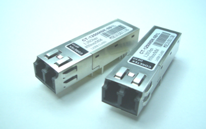
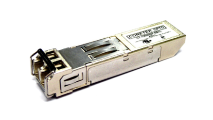
The CT-1250NSP-SB1L-A SFP transceiver is designed for short-reach Gigabit Ethernet, Fibre Channel and high-speed optical interconnects. Its optical interface combines an 850 nm VCSEL transmitter with a multimode receiver in an SFP package. It supports distances up to 550 m over 50/125 µm multimode fibre and 275 m over 62.5/125 µm fibre. The extended case temperature range makes it suitable for equipment operating between −40 and +85 °C. A nominal 3.3 V supply and AC-coupled differential interface support integration with standard SFP host circuits. The duplex LC receptacle provides separate transmit and receive fibre connections. Transmitter disable, transmitter fault, loss-of-signal and two-wire serial identification interfaces are provided through the 20-pin SFP connector.
Range features
A high level overview of what this range offers
- 850 nm VCSEL transmitter – Supports short-reach communication over graded-index multimode fibre.
- 1.25 Gb/s NRZ operation – Suitable for IEEE 802.3z Gigabit Ethernet links.
- 1.06 Gb/s Fibre Channel compatibility – Allows use in supported ANSI Fibre Channel applications.
- Up to 550 m reach – Supports 50/125 µm multimode fibre installations over the stated maximum distance.
- Extended −40 to +85 °C case temperature range – Accommodates equipment exposed to wider operating temperatures.
- 3.3 V supply operation – Aligns with standard SFP host power architectures.
- AC-coupled differential interface – Supports direct connection to compatible high-speed host circuitry.
- Duplex LC receptacle – Provides separate optical transmit and receive paths in a compact connection format.
- SFP MSA interface – Supports integration with mechanically and electrically compatible SFP cages.
- TX_DISABLE, TX_FAULT and RX_LOS functions – Provide host control and link-status monitoring.
- Class 1 laser design – Supports eye-safety requirements under EN 60825-1.
- RoHS-compliant, lead-free construction – Supports restricted-substance requirements for electronic equipment.
Downloads
for CT-1250NSP-SB1L-A 850 nm VCSEL 550 m 1.25 Gb/s SFP Transceiver
What’s in this range?
All the variants in the range and a comparison of what they offer
Specifications
| Category | Specification | Value | Conditions or notes |
|---|---|---|---|
Identification | Model | CT-1250NSP-SB1L-A | Multimode optical transceiver |
Interface | Form factor | SFP | Multi-Source Agreement interface |
Interface | Optical connector | Duplex LC | Separate transmit and receive fibres |
Interface | Electrical coupling | AC/AC differential | Transmit and receive data paths |
Interface | Signal-detect output | TTL | Host status output |
Data | Nominal data rate | 1.25 Gb/s | NRZ signalling |
Data | Fibre Channel rate | 1.06 Gb/s | ANSI Fibre Channel application |
Optical | Transmitter technology | 850 nm VCSEL | Multimode operation |
Optical | Fibre type | 50/125 µm or 62.5/125 µm | Graded-index multimode fibre |
Optical | Maximum distance over 50/125 µm fibre | 550 m | Stated link distance |
Optical | Maximum distance over 62.5/125 µm fibre | 275 m | Stated link distance |
Operating conditions | Nominal supply voltage | 3.3 V | Single supply |
Operating conditions | Supply voltage range | 3.1 to 3.5 V | Normal operation |
Operating conditions | Case temperature | −40 to +85 °C | Extended operating range |
Operating conditions | Data input voltage swing | 400 to 1,660 mV | Differential input |
Absolute ratings | Storage temperature | −40 to +85 °C | Absolute maximum range |
Absolute ratings | Supply voltage | 0 to 6 V | Absolute maximum rating; not an operating range |
Absolute ratings | Supply current | 240 mA maximum | Combined absolute maximum |
Electrical | Transmitter supply current | 140 mA maximum | Transmitter section |
Electrical | Receiver supply current | 100 mA maximum | Receiver section |
Electrical | TX_DISABLE low input | 0 to 0.8 V | Transmitter enabled state |
Electrical | TX_DISABLE high input | 2.0 V to Vcc | High or open disables the module |
Electrical | TX_FAULT low output | 0 to 0.8 V | Fault output low level |
Electrical | TX_FAULT high output | 2.0 V to Vcc | Fault output high level |
Electrical | Receiver differential output voltage | 0.4 to 1.3 V | RD+ and RD− output |
Electrical | RX_LOS low output | 0 to 0.8 V | Loss-of-signal output low level |
Electrical | RX_LOS high output | 2.0 V to Vcc | Loss-of-signal output high level |
Electrical | MOD-DEF low level | −0.6 V to 0.3 × Vcc | Two-wire serial interface |
Electrical | MOD-DEF high level | 0.7 × Vcc to Vcc + 0.5 V | Two-wire serial interface |
Transmitter optical | Average optical output power | −9.5 to −4 dBm | Coupled into specified multimode fibre |
Transmitter optical | Extinction ratio | 9 dB | Specified value |
Transmitter optical | Centre wavelength | 830 to 860 nm | 850 nm typical |
Transmitter optical | RMS spectral width | 0.85 nm | Specified maximum value |
Transmitter optical | Relative intensity noise | −117 dB/Hz | Specified value |
Transmitter optical | Coupled power ratio | 9 dB | Measured in accordance with EIA/TIA-526-14A |
Transmitter optical | Optical rise time | 260 ps | 20–80% value |
Transmitter optical | Optical fall time | 260 ps | 20–80% value |
Transmitter optical | Output eye | IEEE 802.3z/D5.0 compliant | Optical eye requirement |
Receiver optical | Maximum input optical power | −3 dBm | Receiver overload limit |
Receiver optical | Minimum input optical power | ≤ −17 dBm | Measured with 2^7−1 PRBS at BER below 10^−12 |
Receiver optical | Operating wavelength | 770 to 860 nm | Receiver optical range |
Receiver optical | Optical return loss | 12 dB | Specified value |
Receiver optical | Electrical 3 dB upper cut-off frequency | 1,500 MHz | Receiver path |
Receiver optical | LOS asserted threshold | −30 dBm | PA value |
Receiver optical | LOS deasserted threshold | −17 dBm | PD value |
Receiver optical | LOS hysteresis | 0.5 dB | PD minus PA specification |
Timing | TX_DISABLE assert time | 10 µs maximum | Transmitter switch-off response |
Timing | TX_DISABLE negate time | 1 ms maximum | Transmitter switch-on response |
Timing | Initialisation time | 300 ms maximum | Includes TX_FAULT reset |
Timing | Fault-to-TX_FAULT assertion | 100 µs maximum | Fault response |
Timing | TX_DISABLE reset start time | 10 µs maximum | Reset timing |
Timing | RX_LOS assertion time | 100 µs maximum | Off-to-on transition |
Timing | RX_LOS deassertion time | 100 µs maximum | On-to-off transition |
Compliance | Gigabit Ethernet | IEEE 802.3z | 1.25 Gb/s application |
Compliance | Fibre Channel | ANSI Fibre Channel | 1.06 Gb/s application |
Compliance | Laser safety | Class 1, EN 60825-1 | Eye-safety design |
Compliance | Environmental | RoHS compliant and lead-free | Restricted-substance status |
Compliance | Reliability reference | Telcordia GR-468-CORE | Characteristics evaluated against the stated specification |
Compliance | EMC design target | FCC Class B limits | Final equipment compliance remains system dependent |
Pin assignment
| Pin | Symbol | Function |
|---|---|---|
1 | VeeT | Transmitter ground |
2 | TX Fault | Transmitter fault indication |
3 | TX Disable | Transmitter disable; high or open disables the module |
4 | MOD-DEF(2) | Two-wire serial identification interface |
5 | MOD-DEF(1) | Two-wire serial identification interface |
6 | MOD-DEF(0) | Grounded within the module |
7 | Rate Select | Not connected |
8 | LOS | Loss-of-signal indication |
9 | VeeR | Receiver ground |
10 | VeeR | Receiver ground |
11 | VeeR | Receiver ground |
12 | RD− | Inverted received-data output |
13 | RD+ | Received-data output |
14 | VeeR | Receiver ground |
15 | VccR | Receiver power |
16 | VccT | Transmitter power |
17 | VeeT | Transmitter ground |
18 | TD+ | Transmitter data input |
19 | TD− | Inverted transmitter data input |
20 | VeeT | Transmitter ground |
FAQs
for CT-1250NSP-SB1L-A 850 nm VCSEL 550 m 1.25 Gb/s SFP Transceiver
The CT-1250NSP-SB1L-A supports distances up to 550 m over 50/125 µm multimode fibre and 275 m over 62.5/125 µm multimode fibre. It uses an 850 nm VCSEL with an optical output range of −9.5 to −4 dBm and a receiver sensitivity of −17 dBm or better. The difference between the weakest specified transmitter output and receiver sensitivity is 7.5 dB. This figure is the unallocated optical power difference rather than a complete channel budget, so connector loss, splice loss, modal effects and ageing allowances must still be considered. The installed fibre type and channel loss should therefore be verified before the maximum distance is adopted in a design.
Yes, the module is intended for IEEE 802.3z Gigabit Ethernet at 1.25 Gb/s and ANSI Fibre Channel links operating at 1.06 Gb/s. The electrical interface uses NRZ signalling, so the host serializer and receiver circuitry must provide the correct line rate for the selected protocol. Pin 7, which is assigned as Rate Select in the SFP connector format, is not connected in this module. The transceiver should therefore be treated as a fixed-function optical device rather than a host-controlled multi-rate module. Link compatibility still depends on the host port, protocol configuration, optical budget and multimode fibre characteristics.
The module requires a nominal 3.3 V supply and is specified to operate from 3.1 to 3.5 V. Maximum transmitter and receiver supply currents are 140 mA and 100 mA respectively, giving a combined stated maximum of 240 mA. The host power rail and filtering network should be designed above this requirement with an appropriate engineering margin. The differential data input accepts a voltage swing from 400 to 1,660 mV, while the receiver differential output is specified from 0.4 to 1.3 V. The 6 V absolute maximum rating must not be interpreted as an allowable operating voltage, as normal operation is restricted to the 3.1–3.5 V range.
The receiver sensitivity is specified at −17 dBm or better, while the maximum optical input power is −3 dBm. These limits define a 14 dB span between the sensitivity threshold and overload level. The transmitter output ranges from −9.5 to −4 dBm, leaving 1 dB between the strongest specified transmitter output and the receiver overload limit before channel losses are introduced. Very short laboratory or equipment-level links should still be checked for measurement tolerance and unexpected power variation. At the weak-signal end, the −17 dBm sensitivity is associated with a 2^7−1 test pattern and a bit error rate below 10^−12, so production testing should use equivalent acceptance criteria where required.
TX_DISABLE is active high, and leaving the input open also disables the transmitter. A low level is defined between 0 and 0.8 V, while a high level extends from 2.0 V to Vcc. TX_FAULT provides a transmitter fault indication, and RX_LOS reports insufficient received optical power using TTL-compatible output levels. The specified LOS thresholds are −30 dBm for assertion and −17 dBm for deassertion, with 0.5 dB of stated hysteresis. Host firmware should also account for the timing limits, including up to 300 ms for initialisation, 10 µs for TX_DISABLE assertion and 100 µs for RX_LOS assertion or deassertion.
The specified case operating temperature is −40 to +85 °C, and the storage temperature range is also −40 to +85 °C. The operating limit applies to the module case, so enclosure ambient temperature alone is not sufficient for thermal validation. Airflow, cage temperature, neighbouring heat sources and the module’s combined current consumption must be included when assessing the thermal design. The optical transmitter is designed for Class 1 operation under EN 60825-1, while the construction is identified as RoHS compliant and lead-free. EMC behaviour is designed around FCC Class B limits, although the completed host equipment still requires system-level emissions and immunity assessment.
The module uses the SFP form factor, a 20-pin electrical connector and a duplex LC optical receptacle. Integration therefore requires a compatible SFP cage, host connector and transmit and receive fibre arrangement. The high-speed electrical paths are provided through TD+/TD− and RD+/RD− differential pairs, with separate transmitter and receiver power and ground pins. Rate Select is not connected, while MOD-DEF(0), MOD-DEF(1) and MOD-DEF(2) support module presence and serial identification functions. PCB routing should maintain the intended differential impedance, minimise discontinuities and use suitable supply filtering close to the cage connection.
Digital diagnostic monitoring is not specified for the CT-1250NSP-SB1L-A. The MOD-DEF(1) and MOD-DEF(2) pins are assigned to a two-wire serial identification interface, but that assignment alone does not confirm support for real-time temperature, voltage, bias-current or optical-power telemetry. A host design should not assume compatibility with DDM or DOM management functions. Link supervision can still use the dedicated RX_LOS and TX_FAULT outputs, together with transmitter control through TX_DISABLE. If live optical and electrical telemetry is mandatory, that capability should be confirmed before the module is approved for the application.