DHPVA 100/200 MHz Wideband Voltage Amplifier
- Technology
- Amplifiers
- Partner
- FEMTO Messtechnik
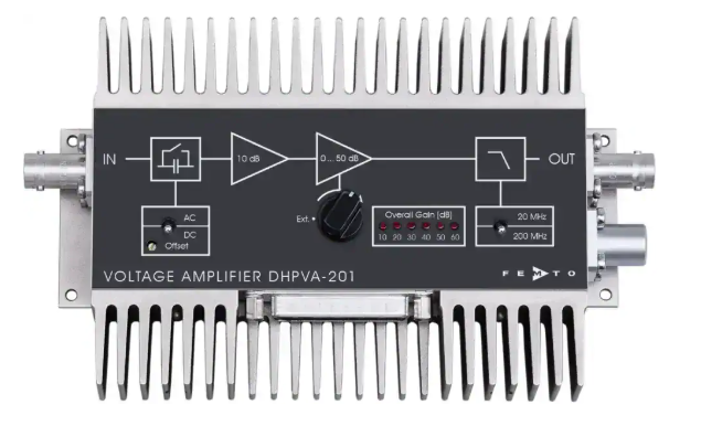
The DHPVA-101 and DHPVA-201 are variable-gain wideband voltage amplifiers for measuring low-level signals at frequencies extending into the MHz range. Both models provide gain settings from 10 to 60 dB in 10 dB steps, allowing one amplifier to accommodate changing signal levels. Bandwidth and rise/fall time vary by no more than ±10% across the complete gain range, supporting consistent time-resolved measurements when sensitivity is changed. Switchable AC/DC coupling and reduced-bandwidth modes provide control over baseline response and integrated wideband noise. The DHPVA-101 offers full and reduced bandwidths of 100 MHz and 10 MHz, while the DHPVA-201 provides 200 MHz and 20 MHz.
Typical applications include oscilloscope and transient-recorder preamplification, photomultiplier and microchannel-plate amplification, optical receiver signal boosting and automated measurement equipment. Local controls and opto-isolated TTL/CMOS-compatible inputs support manual, remote or mixed operation. The current DHPVA-101 and DHPVA-201 variants maintain compatibility with the earlier DHPVA-100 and DHPVA-200 models.
Range features
A high level overview of what this range offers
- Six gain settings from 10 to 60 dB: Adapts the output level to different source amplitudes without changing amplifiers.
- Gain-independent bandwidth within ±10%: Supports comparable pulse timing and frequency response when gain is adjusted.
- DC or 10 Hz lower cut-off frequency: Allows direct baseline measurement or suppression of low-frequency and DC components.
- Selectable 10/100 MHz or 20/200 MHz bandwidth: Balances signal speed against integrated wideband noise.
- Approximately Bessel reduced-bandwidth response: Supports controlled pulse response in the filtered mode.
- 2.3 nV/√Hz input voltage noise at 30–60 dB gain: Supports measurement of small input signals within an appropriately limited bandwidth.
- 0.3 µV/°C input voltage drift: Reduces temperature-related offset movement in DC measurements.
- Adjustable ±10 mV input offset range: Enables local or externally controlled baseline correction.
- 50 Ω BNC input and output: Integrates directly into standard RF and high-speed measurement paths.
- 2 Vpp linear output range: Provides up to +10 dBm output power with a maximum output current of 70 mA.
- DC to 100 kHz monitor output: Provides a separate low-frequency representation of the signal for monitoring or control tasks.
- Local and opto-isolated remote control: Supports manual operation, automated test equipment and mixed local/remote configurations.
- Input-signal envelope from about 100 µV to 300 mV: Covers a 70 dB range, extending to roughly 10 µV with signal averaging.
- Compatibility with DHPVA-100 and DHPVA-200: Supports replacement within existing measurement arrangements.
What’s in this range?
All the variants in the range and a comparison of what they offer
Common series specifications
| Category | Parameter | Specification |
|---|---|---|
Test conditions | Electrical specification conditions | Supply ±15 V, ambient temperature 25 °C, system impedance 50 Ω |
Gain | Switchable gain values | 10, 20, 30, 40, 50 and 60 dB |
Gain | Approximate voltage gain | ×3 to ×1,000 |
Gain | Gain accuracy | ±0.15 dB |
Frequency response | Lower cut-off frequency | DC or 10 Hz, switchable |
Input | Input impedance | 50 Ω |
Input | Equivalent input voltage noise | 2.3 nV/√Hz at 30–60 dB gain |
Input | Equivalent input current noise | 3.0 pA/√Hz |
Input | 1/f noise corner | 20 kHz |
Input | Input voltage drift | 0.3 µV/°C |
Input | Input bias current | Less than 200 nA |
Input | Input offset voltage | −10 mV to +10 mV, adjustable locally or by external control voltage |
Output | Output impedance | 50 Ω; use a 50 Ω load for the stated main-output performance |
Output | Linear output voltage range | 2 Vpp, equivalent to approximately ±1 V about zero |
Output | Maximum output power | +10 dBm |
Output | Maximum output current | 70 mA |
Monitor output | Voltage gain | ×1 with a load of at least 1 MΩ |
Monitor output | Voltage range | ±5 V |
Monitor output | Output current | ±10 mA |
Monitor output | Bandwidth | DC to 100 kHz |
Monitor output | Output impedance | 50 Ω, designed for a load of at least 1 MΩ |
Indication | LED function | Displays the selected gain setting |
Digital control | Control inputs | Five opto-isolated inputs, TTL/CMOS compatible |
Digital control | Logic-low voltage | −0.8 to +0.8 V |
Digital control | Logic-high voltage | +1.8 to +12 V |
Digital control | Input current | 0 mA at 0 V, 1.5 mA at +5 V and 4.5 mA at +12 V |
Digital control | Gain switching time | 5 ms |
External offset control | Control voltage | ±10 V, corresponding to ±10 mV input offset |
External offset control | Input impedance | 20 kΩ |
Power | Supply voltage | ±15 V |
Power | Supply current | ±120 mA typical; ±400 mA maximum |
Power | Auxiliary outputs | ±12 V at 50 mA maximum and +5 V at 50 mA maximum |
Case | Weight | 560 g |
Case | Material | Nickel-plated AlMg4.5Mn |
Temperature | Operating range | 0 °C to +50 °C |
Temperature | Storage range | −40 °C to +85 °C |
Absolute maximum | Supply voltage | ±16.5 V |
Absolute maximum | Signal input voltage | ±5 V |
Absolute maximum | Digital control input | +16 V / −5 V |
Signal connectors | Input and output | Female BNC |
Power connector | Type | Three-pin series 1S fixed socket; mating plug type FFA.1S.303.CLAC52 |
Control connector | Type | Female 25-pin D-sub, quality class 2 |
Protection | Main output | Short-circuit protected |
Variant comparison
| Specification | DHPVA-101 | DHPVA-201 |
|---|---|---|
Full/reduced upper cut-off frequency | 100 MHz / 10 MHz | 200 MHz / 20 MHz |
Lower cut-off frequency | DC / 10 Hz, switchable | DC / 10 Hz, switchable |
Gain settings | 10/20/30/40/50/60 dB | 10/20/30/40/50/60 dB |
Input voltage noise | 2.3 nV/√Hz | 2.3 nV/√Hz |
Input voltage drift | 0.3 µV/°C | 0.3 µV/°C |
Rise/fall time at full bandwidth | 3.5 ns at 100 MHz | 1.8 ns at 200 MHz |
Rise/fall time at reduced bandwidth | 35 ns at 10 MHz | 18 ns at 20 MHz |
Input return loss S11 | −37 dB at 50 MHz; −31 dB at 100 MHz; −21 dB at 200 MHz | −31 dB at 100 MHz; −22 dB at 200 MHz; −10 dB at 400 MHz |
Output return loss S22 | −40 dB at 50 MHz; −35 dB at 100 MHz; −31 dB at 200 MHz | −35 dB at 100 MHz; −30 dB at 200 MHz; −25 dB at 400 MHz |
Output voltage and power | 2 Vpp; +10 dBm maximum | 2 Vpp; +10 dBm maximum |
Total harmonic distortion | Less than 0.5% at 10 MHz and 1 Vpp | Less than 0.5% at 20 MHz and 1 Vpp |
Monitor output | DC to 100 kHz | DC to 100 kHz |
Digital interface | Opto-isolated TTL/CMOS inputs | Opto-isolated TTL/CMOS inputs |
Bandwidth control on Pin 14 | Low: 10 MHz; high: 100 MHz | Low: 20 MHz; high: 200 MHz |
Compatible earlier model | DHPVA-100 | DHPVA-200 |
Remote-control inputs are combined with the local switch positions by logical OR. The relevant local control must be placed in its external-control, AC or reduced-bandwidth position before the associated digital input can select the required setting.
Remote-control logic
| Control function | Selection | Pin or pins | Logic state |
|---|---|---|---|
Gain | 10 dB | Pins 10/11/12 | Low / low / low |
Gain | 20 dB | Pins 10/11/12 | High / low / low |
Gain | 30 dB | Pins 10/11/12 | Low / high / low |
Gain | 40 dB | Pins 10/11/12 | High / high / low |
Gain | 50 dB | Pins 10/11/12 | Low / low / high |
Gain | 60 dB | Pins 10/11/12 | High / low / high |
Coupling | AC | Pin 13 | Low |
Coupling | DC | Pin 13 | High |
Bandwidth | Reduced: 10 MHz or 20 MHz | Pin 14 | Low |
Bandwidth | Full: 100 MHz or 200 MHz | Pin 14 | High |
FAQs
for DHPVA 100/200 MHz Wideband Voltage Amplifier
Choose the model according to the highest signal frequency and shortest edge time that the measurement must retain. The DHPVA-101 provides 100 MHz full bandwidth with a 3.5 ns rise/fall time, while its reduced mode provides 10 MHz and 35 ns. The DHPVA-201 extends these values to 200 MHz and 1.8 ns, with a 20 MHz reduced mode giving an 18 ns response. Both models otherwise share the same gain range, input noise, drift, 50 Ω signal path and control arrangement. The 200 MHz version is therefore appropriate when the additional bandwidth is required, whereas the 100 MHz model covers systems whose useful spectrum remains below that limit.
Select the lowest gain that gives adequate digitiser or oscilloscope resolution while keeping the amplifier output below its 2 Vpp linear range. The available 10, 20, 30, 40, 50 and 60 dB settings correspond to voltage gains of approximately ×3.16, ×10, ×31.6, ×100, ×316 and ×1,000. For example, a 10 mVpp input produces about 1 Vpp at 40 dB, while 50 dB would target approximately 3.16 Vpp and exceed the linear range. The usable input-signal envelope is about 100 µV to 300 mV, extending towards 10 µV when averaging is applied. Actual resolution at the lower end also depends on measurement bandwidth, source impedance and the required signal-to-noise ratio.
Gain-independent bandwidth means that changing sensitivity does not produce the usual large change in edge speed or frequency response. Bandwidth and rise/fall time remain within a maximum deviation of ±10% across the six gain settings, allowing measurements at different gains to be compared more directly. At full bandwidth, the nominal rise/fall times are 3.5 ns for the DHPVA-101 and 1.8 ns for the DHPVA-201. The reduced modes change these times to 35 ns and 18 ns respectively and use an approximately Bessel response. This lets the engineer retain full speed for fast transients or intentionally limit bandwidth when reduced integrated noise is more important.
Use DC coupling when the absolute signal level, slow variations or frequencies below 10 Hz must be measured. AC coupling introduces a 10 Hz lower cut-off, making it suitable when a DC component or slow baseline movement would otherwise consume output range. In DC mode, the input offset can be adjusted across −10 mV to +10 mV using the front control or an external voltage. The external ±10 V control range corresponds to ±10 mV of input-referred offset adjustment, while the input voltage drift is 0.3 µV/°C. The coupling choice should therefore be based on whether baseline information is required and how much offset can be tolerated within the selected gain and output range.
Yes, five opto-isolated digital inputs provide remote control of gain, coupling and bandwidth using TTL/CMOS-compatible levels. Logic low is defined from −0.8 to +0.8 V, while logic high is accepted from +1.8 to +12 V. Gain is coded through Pins 10 to 12, AC/DC coupling uses Pin 13 and the bandwidth mode uses Pin 14, with a stated gain-switching time of 5 ms. The remote bits operate by logical OR with the local switches, so the corresponding local control must first be placed in the required remote-compatible position. Mixed operation is also possible, allowing gain to remain under local control while bandwidth or coupling is managed by the test system.
The main input and output are both designed for a 50 Ω environment and use female BNC connectors. A 50 Ω RF cable and a 50 Ω receiving termination should be used when the specified bandwidth, pulse response and return-loss performance are required. At 100 MHz, the DHPVA-101 has input and output return losses of −31 dB and −35 dB respectively; at 200 MHz, the DHPVA-201 values are −22 dB and −30 dB. The separate monitor output also has a 50 Ω source impedance, but it is designed to drive a load of at least 1 MΩ. Terminating that monitor connection in 50 Ω would therefore reduce its available voltage and would not represent its intended operating condition.
The amplifier requires a regulated ±15 V supply through its three-pin power connector. Typical supply current is ±120 mA, although the maximum rating is ±400 mA depending on operating conditions. The specified operating temperature range is 0 °C to +50 °C, with storage permitted from −40 °C to +85 °C. One or both heat sinks may be removed only when the enclosure or rack provides an alternative thermal path below 2 K/W through suitable metal-to-metal contact. For an integrated system, the designer should therefore allow for supply headroom, connector access, airflow and a defined conductive cooling path before changing the standard heat-sink arrangement.